Method and apparatus for tuning phase of clock signal

a clock signal and phase technology, applied in the field of semiconductor devices, can solve the problems of increasing the speed, limiting the frequency of the main clock signal, and limiting the data interface speed with respect to the core speed of the dram, so as to achieve the effect of more rapid tuning

Active Publication Date: 2011-03-08
SAMSUNG ELECTRONICS CO LTD
View PDF18 Cites 23 Cited by
  • Summary
  • Abstract
  • Description
  • Claims
  • Application Information

AI Technical Summary

Benefits of technology

[0008]It is therefore a separate feature of an embodiment to provide a method and apparatus for more quickly tuning a phase of a data clock signal or a frequency-divided signal of the data clock signal, which has a different frequency than a main clock signal, to a phase of the main clock signal in a semiconductor memory apparatus.

Problems solved by technology

However, since it is very difficult to increase the speed due to the structure of the core circuit in the DRAM, there is a limit to increasing the frequency of the main clock signal.
However, there is a limit to increasing the data interface speed with respect to the core speed of the DRAM while the main clock signal and the data strobe signal are maintained to have the same frequency in the DRAM.

Method used


Image

  • Method and apparatus for tuning phase of clock signal
  • Method and apparatus for tuning phase of clock signal
  • Method and apparatus for tuning phase of clock signal

Examples


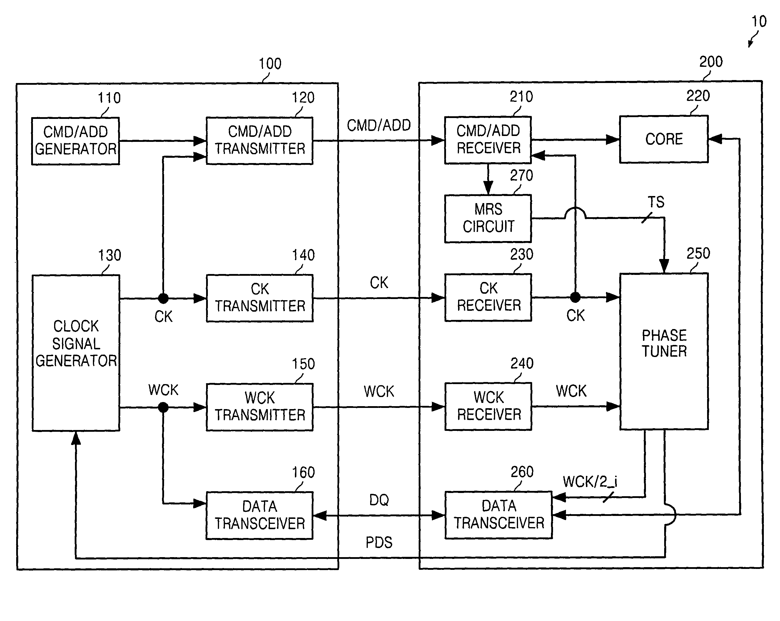
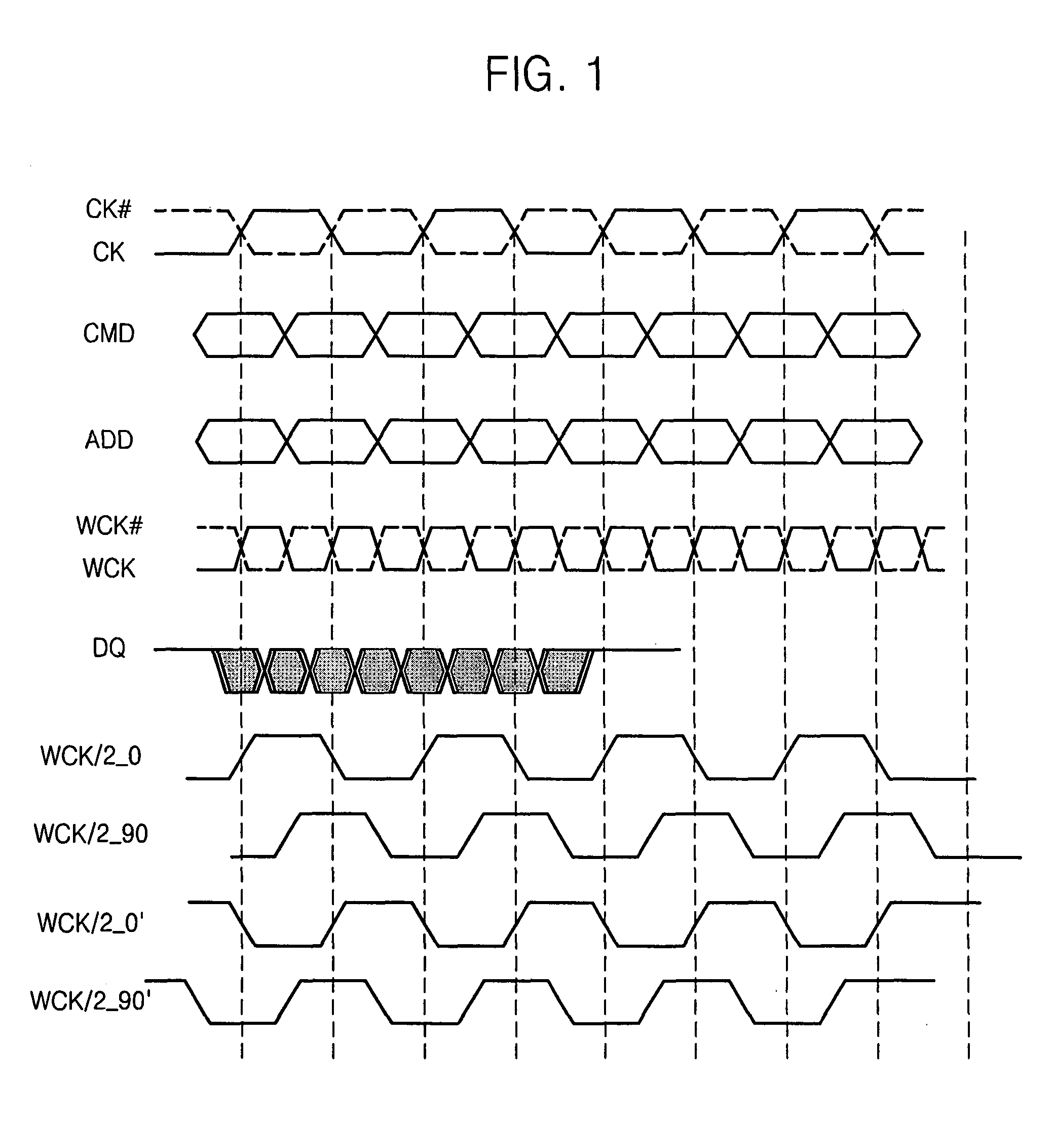
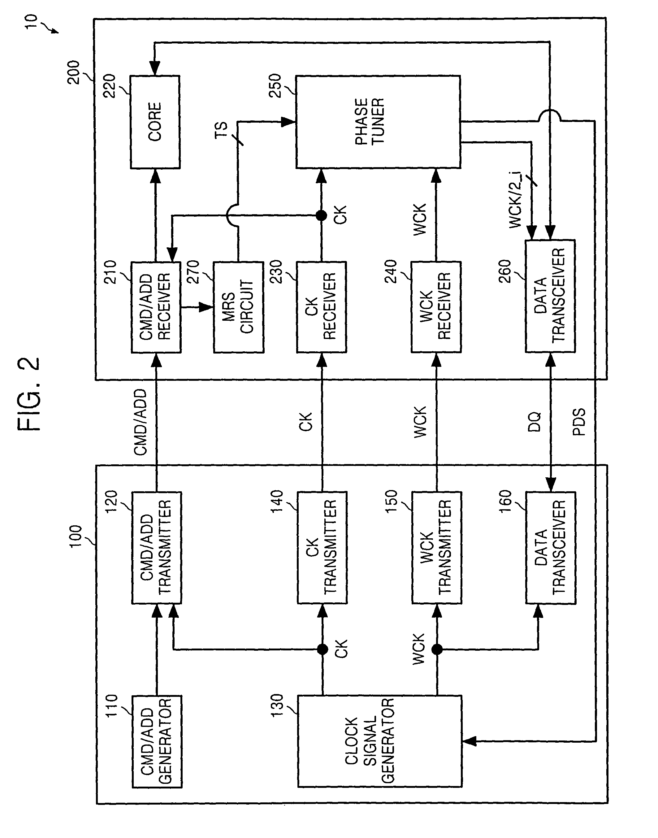
Embodiment Construction

[0044]Korean Patent Application No. 10-2008-0032459, filed on Apr. 8, 2008, in the Korean Intellectual Property Office, and entitled: “Method and Apparatus for Tuning Phase of Clock Signal,” is incorporated by reference herein in its entirety.

[0045]Exemplary embodiments will now be described more fully hereinafter with reference to the accompanying drawings; however, they may be embodied in different forms and should not be construed as limited to the embodiments set forth herein. Rather, these embodiments are provided so that this disclosure will be thorough and complete, and will fully convey the scope of the invention to those skilled in the art. In the drawings, the size and relative sizes of layers and regions may be exaggerated for clarity. Like numbers refer to like elements throughout the specification.

[0046]It will be understood that when an element is referred to as being “connected” or “coupled” to another element, it can be directly connected or coupled to the other elem...


PUM


Abstract

A method and apparatus for tuning a phase of a data clock signal having a different frequency than a main clock signal. The method of tuning includes coarse tuning by receiving the data clock signal, dividing the data clock signal to generate a frequency-divided clock signal having a same frequency as the main clock signal, repeatedly shifting the frequency-divided clock signal to generate multiphase frequency-divided clock signals at a predetermined phase interval, comparing a phase of each of the multiphase frequency-divided clock signals with a phase of the main clock signal, and determining a phase shift amount based on a comparison result, and fine tuning by comparing a phase of a multiphase frequency-divided clock signal corresponding to the phase shift amount with the phase of the main clock signal and adjusting the phase of the data clock signal by a predetermined phase step based on the comparison result.

Description

BACKGROUND[0001]1. Field[0002]Embodiments relate to a semiconductor apparatus, and more particularly, to a method and circuit for tuning the phase of a data clock signal used to input and output data in a semiconductor apparatus.[0003]2. Description of the Related Art[0004]Dynamic random access memory (DRAM), for example, DDR1 / 2 / 3 and GDDR3 / 4, usually performs a core operation using a main clock signal and interfaces with a memory controller using a data strobe signal. In other words, data is transmitted in synchronization with the data strobe signal. The main operation of the core operation is accessing a memory cell array, i.e., a core of the DRAM, that is, writing data to or reading data from the memory cell array. At this time, the main clock signal and the data strobe signal have the same frequency. Therefore, when data is transmitted at a rising edge and a falling edge of the data strobe signal, the data is transmitted at a double data rate (DDR) with respect to the main clock...

Claims


Application Information

Patent Timeline
Patent Type & Authority Patents(United States)
IPC IPC(8): H03L7/06
CPCG11C7/22G11C7/222H03L7/06G11C2207/2254G06F13/16G11C11/4076
Inventor BAE, SEUNG JUNPARK, KWANG ILBANG, SAM YOUNGMOON, GIL SHINYEOM, KI WOONG
Owner SAMSUNG ELECTRONICS CO LTD
Why Eureka
Try Eureka