

Receiving circuit and method for compensating IQ mismatch
a receiving circuit and receiver technology, applied in the direction of receiver monitoring, transmission monitoring, synchronous/start-stop system, etc., can solve the problems of iq mixer gain error generation, receiver performance degradation,
- Summary
- Abstract
- Description
- Claims
- Application Information
AI Technical Summary
Benefits of technology
Problems solved by technology
Method used
Image

Examples
seventh embodiment
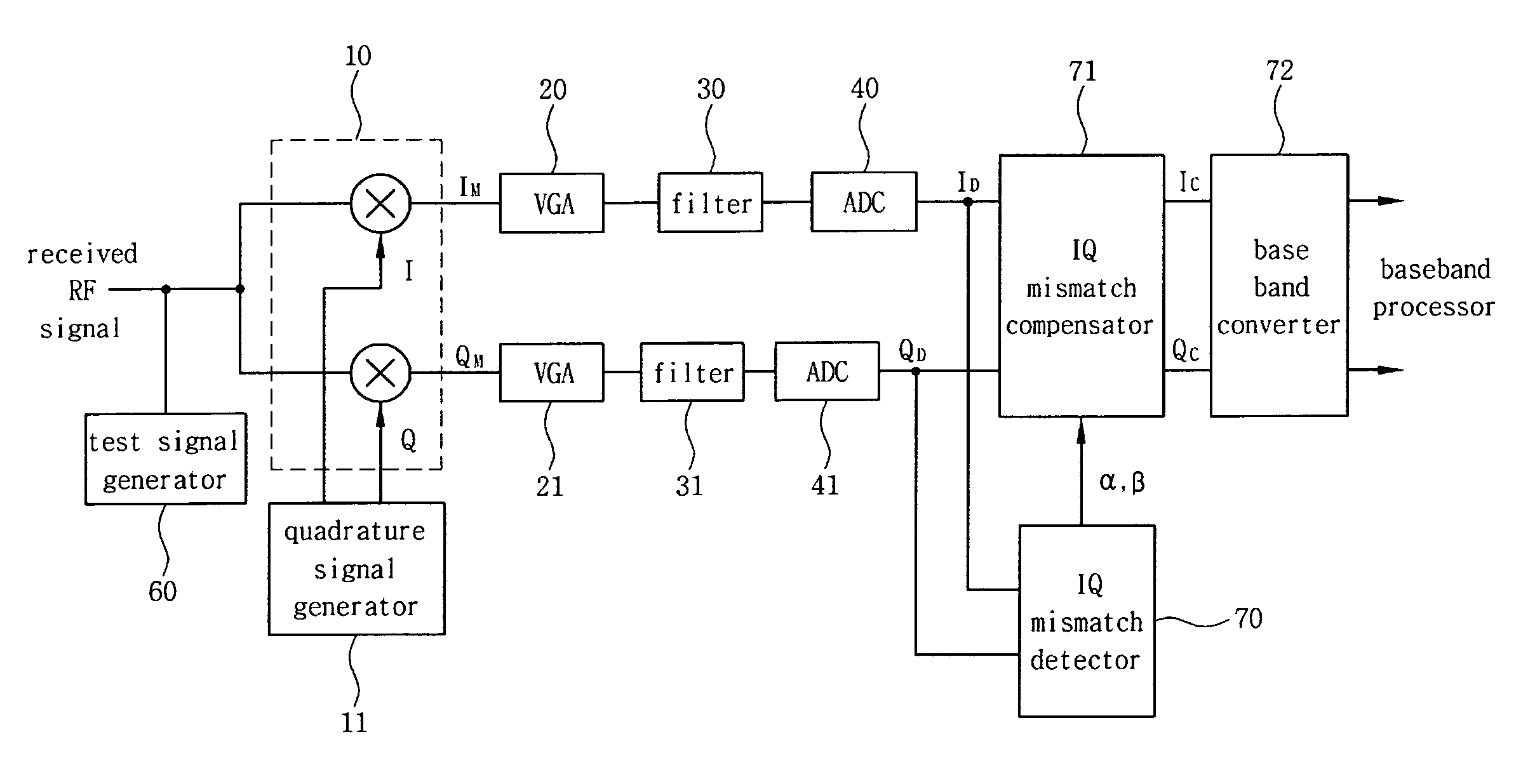
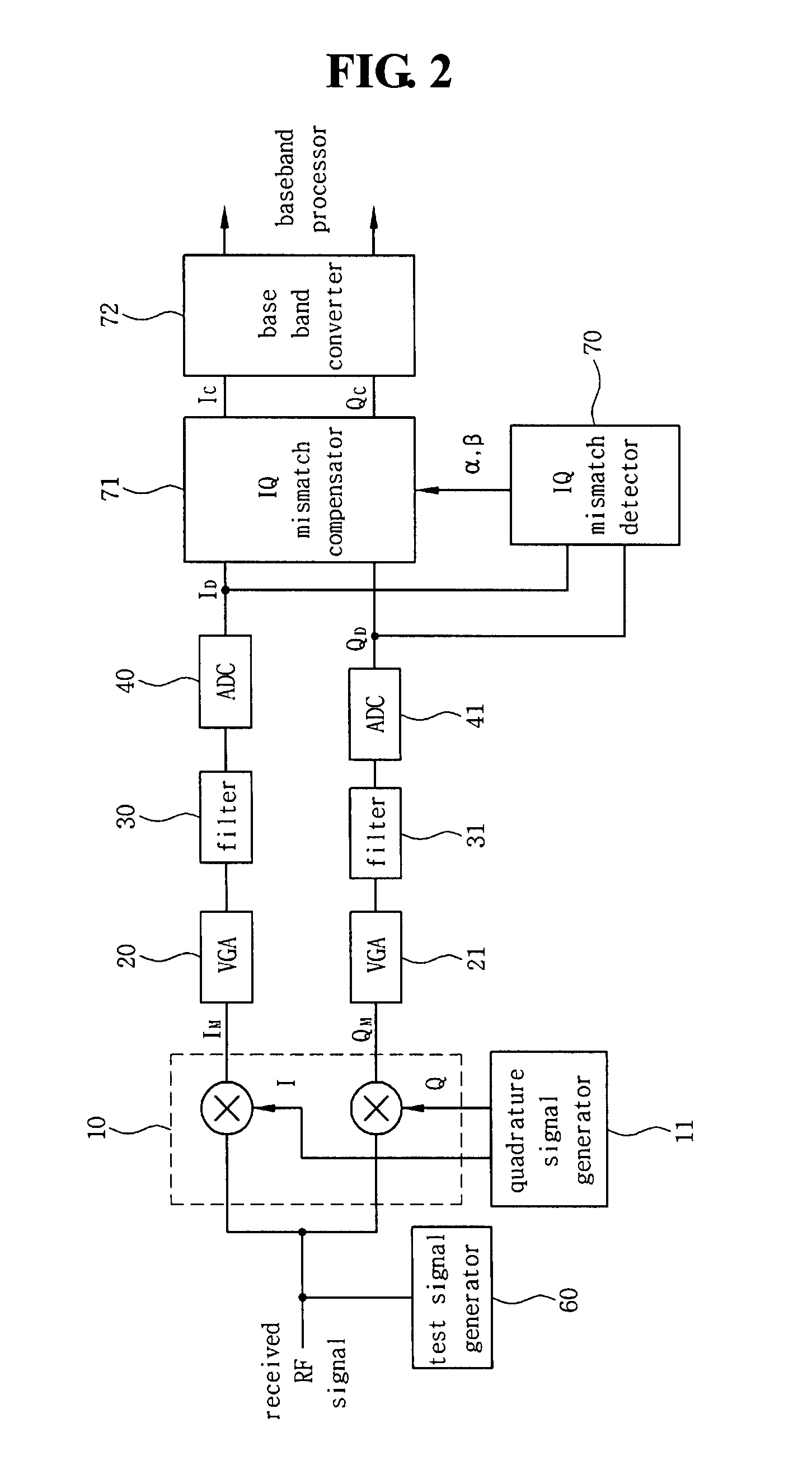
[0063]FIG. 13 is a flowchart illustrating a method for compensating for an IQ mismatch in accordance with a seventh embodiment according to the invention. As shown in FIG. 13, after a process starts a method for compensating for an IQ mismatch can include converting a sum of a received signal and a test signal positioned in a guard band to a first signal and a second signal of an intermediate frequency or a base band using an IQ mixer (block S1), detecting the IQ mismatch using the test signal included in a third signal and a fourth signal corresponding to the first signal and the second signal (block S2), and compensating for the IQ mismatch using the IQ mismatch detected (block S3).
[0064]When the sum of the received RF signal and the test signal positioned in the guard band is converted to the first signal and the second signal of the intermediate frequency (block S1), it is preferable that the received RF signal includes a desired signal and an interference signal for generating ...
eighth embodiment
[0068]FIG. 14 is a flowchart illustrating a method for compensating for an IQ mismatch in accordance with an eighth embodiment according to the invention. As shown in FIG. 14, a method for compensating for an IQ mismatch can include converting a sum of a received signal and a test signal positioned in a guard band to a first signal and a second signal of an intermediate frequency or a base band using an IQ mixer (block S11), outputting a fifth signal and a sixth signal according to a signal corresponding to a gain error and a signal corresponding to a phase error, wherein the fifth signal and the sixth signal are obtained by compensating for the IQ mismatch the third signal and the fourth signal corresponding to the first signal and the second signal (block S12), and obtaining the signal corresponding to the gain error and the signal corresponding to the phase error using the test signal included in the fifth signal and the sixth signal (block S13).
[0069]In one embodiment, the sum o...
PUM
 Abstract
Description
Claims
Application Information