Method for forming trench and method for fabricating semiconductor device using the same

a technology of trenches and semiconductors, applied in the direction of semiconductor devices, electrical equipment, basic electric elements, etc., can solve the problems of field oxide layer loss, trench sidewall passivation effect decrease,

Inactive Publication Date: 2011-07-19
SK HYNIX INC
View PDF17 Cites 221 Cited by
  • Summary
  • Abstract
  • Description
  • Claims
  • Application Information

AI Technical Summary

Problems solved by technology

In a recess gate process currently used, however, an etch barrier layer used in etching the substrate to form a trench is an oxide layer, and thus a bowing phenomenon takes place at a sidewall profile of the trench because small amount of byproduct results in the decrease in passivation effect of the trench sidewall (see A of FIG. 1).
However, it is not preferable to use the H2 gas because it is too dangerous.
Further, a field oxide layer may be lost during the etch process of forming the trench for a recess gate (see B of FIG. 1).
In addition to the aforementioned recess gate process, the trench forming process for a semiconductor memory device encounters a great challenge to achieve the effective passivation of the trench sidewall and thus to prevent the bowing phenomenon of the trench sidewall profile during all the processes of forming a trench by selectively etching a substrate, for example, in the case where the trench sidewall for device isolation must be formed vertically in an STI process of a flash memory device.

Method used


Image

  • Method for forming trench and method for fabricating semiconductor device using the same
  • Method for forming trench and method for fabricating semiconductor device using the same
  • Method for forming trench and method for fabricating semiconductor device using the same

Examples


Embodiment Construction

[0014]Embodiments of the present invention relate to a method for forming a trench and a method for fabricating a semiconductor device using the same.

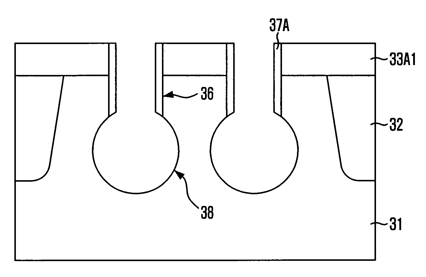
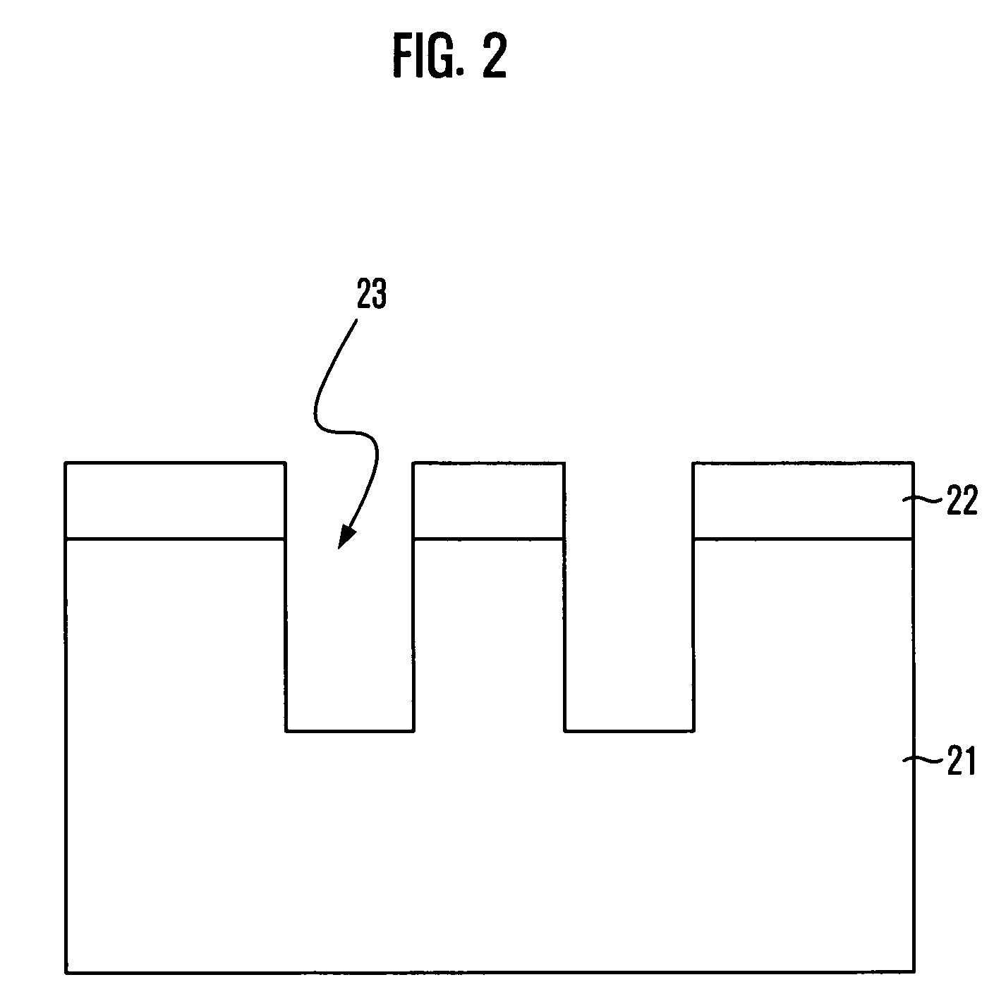
[0015]FIG. 2 is a cross-sectional view of a method for forming a trench in accordance with an embodiment of the present invention. Referring to FIG. 2, a mask pattern 22 is formed over a substrate 21 to expose a region that will be etched. The substrate 21 is etched using the mask pattern 22 as an etch barrier to form a trench 23. The etch process is performed using Cl2 gas as a main etch gas and SiFX as an additive gas, where x is a positive integer. In the case where the etch process is performed using Cl2 gas and SiFX gas to form the trench 23, the trench 23 has a sidewall with a vertical profile by virtue of reaction of the Cl2 gas and the SiFX gas. The reason is that the sidewall of the trench 23 is passivated by a polymer generated from the reaction of the Cl2 gas and the SiFX gas.

[0016]For example, if the SiFX gas is tetrafluoro...


PUM


Abstract

A method for forming a trench includes providing a substrate, and forming the trench in the substrate using a gas containing chlorine (Cl2) gas as a main etch gas and SiFX gas as an additive gas, wherein a sidewall of the trench has a substantially vertical profile by virtue of reaction of the Cl2 gas and the SiFX gas.

Description

CROSS-REFERENCE TO RELATED APPLICATIONS[0001]The present invention claims priority of Korean patent application number 2007-0026542, filed on Mar. 19, 2007, which is incorporated by reference in its entirety.BACKGROUND OF THE INVENTION[0002]The present invention relates to a method for fabricating a semiconductor device, and more particularly, to a method for forming a trench and a method for fabricating a semiconductor device using the same.[0003]Generally, a recess gate process, a shallow trench isolation (STI) process of a flash memory device, or the like, essentially employs a process of forming a trench in a substrate by partially etching the substrate to a predetermined depth. In the forming process of a trench, it is desirable to form the trench such that its sidewalls have a vertical profile for various reasons. For instance, a process of forming a trench for a recess gate will be described hereinafter.[0004]A recess gate process can increase a channel length of a cell trans...

Claims


Application Information

Patent Timeline
Patent Type & Authority Patents(United States)
IPC IPC(8): H01L21/302
CPCH01L21/02057H01L21/3065H01L21/3081H01L21/3083H01L21/76232H01L29/4236H01L29/66621H01L21/18
Inventor JUNG, TAE-WOO
Owner SK HYNIX INC
Why Eureka
Try Eureka