Semiconductor device

a technology of semiconductor devices and circuits, applied in the field of semiconductor devices, can solve the problems of large circuit scale and drop in bus throughput, and achieve the effects of reducing the expansion of the circuit scale of the router, and increasing bus access or data processing

Inactive Publication Date: 2011-07-19
RENESAS ELECTRONICS CORP
View PDF16 Cites 3 Cited by
  • Summary
  • Abstract
  • Description
  • Claims
  • Application Information

AI Technical Summary

Benefits of technology

[0006]The inventor conducted examination about how to suppress the decrease in bus throughput or data-processing throughput owing to the conflict between requests from master components to a slave component, the conflict between responses from slave components to a master component, and the like. With the technique as disclosed by JP-A-2002-342265, which was found after completion of the invention, an attempt is made to use an aggregate circuit for part of master components thereby to reduce the number of specialized busses for the purpose of increasing the efficiency of access to a slave component by a master component by means of multiplexing of access buses. However, even when a bus which the aggregate circuit has assigned to nothing remains, the action to assign the bus to a master component on the side of the aggregate circuit to use is not taken. Further, the scale of the circuit is large because it is premised on multiplexing of buses. The adoption of the crossbar switch circuit as disclosed in JP-A-2000-200258 offers a superior flexibility in the light of deciding a component to connect with, however enlarges the scale of the circuit.
[0008]Hence, it is an object of the invention to provide a semiconductor device which can increase the bus access efficiency while the expansion of circuit scale of the router is suppressed.
[0011]That is, the router which relays a transfer request and a reply between master and slave components has request-control circuits provided therein; the request-control circuits judge the slave component to transfer a request from each master component to, and arbitrate the conflict between requests to one slave component. Further, for the router, a slave-component-allocation-control circuit which variably allocates the request-control circuits the slave components to be connected to the request-control circuits is adopted. In case that a slave component in connection with one request-control circuit is subjected to no access, changing the allocation of the slave component in connection with the one request-control circuit makes possible to utilize the resource of the one request-control circuit, and thus the throughput of bus access or data processing is increased. In addition, this is not predicated on multiplexing of buses, and a crossbar switch covering the whole is not required. Therefore, the expansion of the circuit scale of the router can be minimized.
[0012]Now, the effects offered by the preferred ones of the embodiments herein disclosed are briefly as follows. That is, the expansion of the circuit scale of the router can be minimized, and the efficiency of buss access can be increased.

Problems solved by technology

Further, the scale of the circuit is large because it is premised on multiplexing of buses.
However, the inventor revealed that in the fixed condition, a resource of the router, which the one request-control circuit forms, is not used effectively when a slave component connected to one request-control circuit is subjected to no access at all, and therefore the bus throughput can drop depending on the details of data processing.

Method used


Image

  • Semiconductor device
  • Semiconductor device
  • Semiconductor device

Examples


Embodiment Construction

1. Summary of the Preferred Embodiments

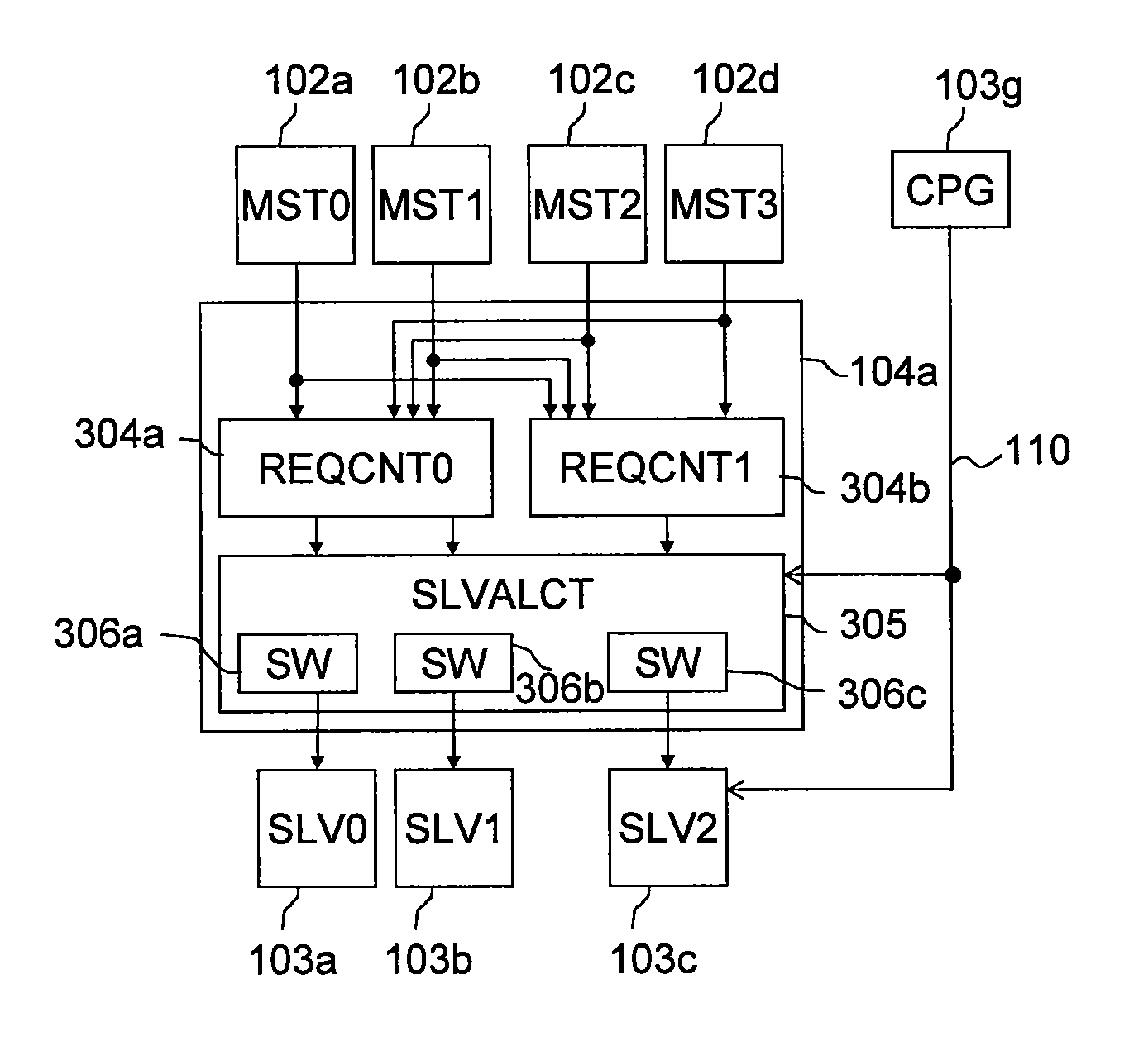
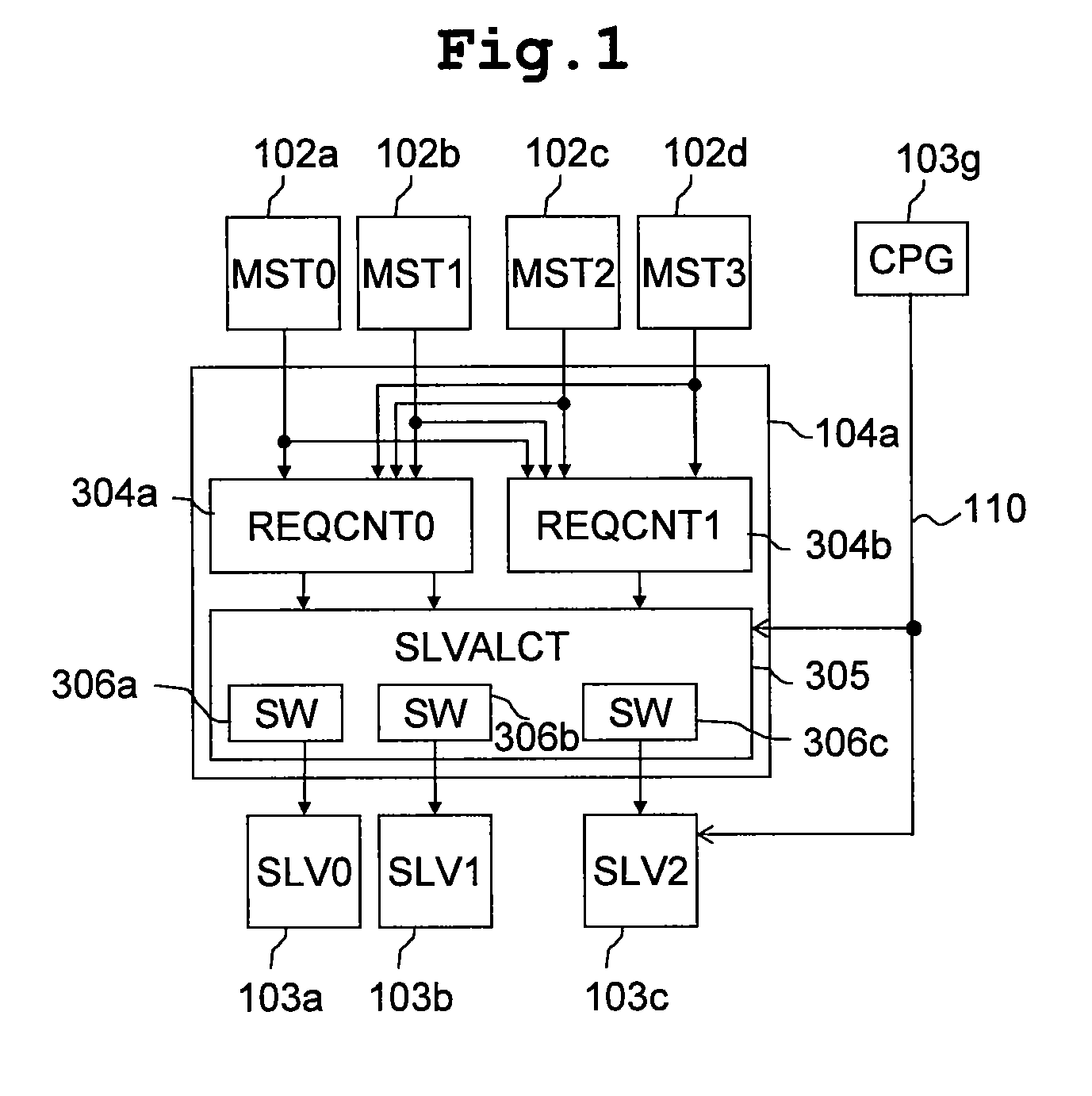
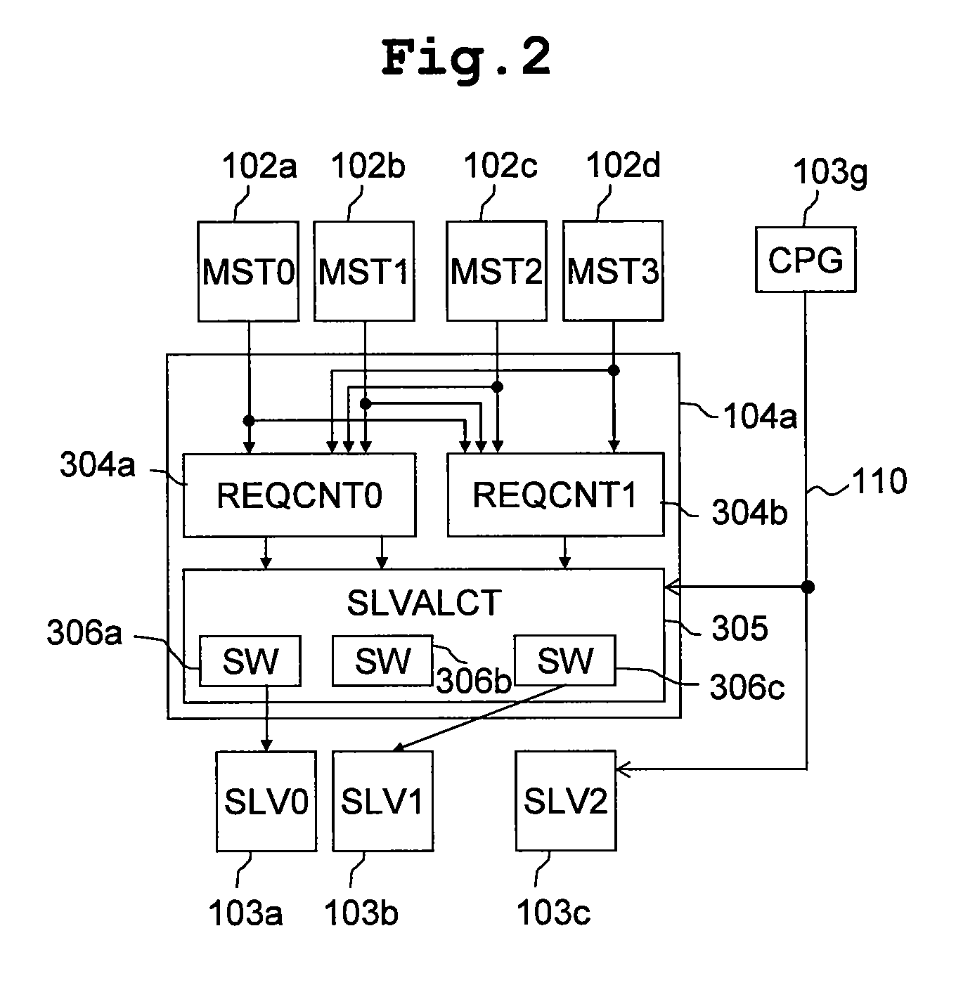
[0027]First, the preferred embodiments of the invention herein disclosed will be described in outline. Here, the reference numerals, characters and signs for reference to the drawings, which are accompanied with paired round brackets, only exemplify what the concepts of components referred to by the numerals, characters and signs contain.

[0028][1] The semiconductor device has a plurality of master components (102a-102f) capable of making a request for transfer; a plurality of slave components (103a-103f) capable of making a reply to the transfer request; and a router (104) which relays the transfer request and reply between the master and slave components. The router has: a plurality of request-control circuits (304, 404) each judging the slave component to transfer a request from each master component to, and arbitrating the conflict between requests to one slave component; and a slave-component-allocation-control circuit (305, 405, 505) varia...


PUM


Abstract

The router which relays a transfer request and a reply between master and slave components has request-control circuits provided therein. The request-control circuits judge the slave component to transfer a request from each master component to, and arbitrate the conflict between requests to one slave component. Further, for the router, a slave-component-allocation-control circuit which variably allocates the slave components to be connected to the request-control circuits to the request-control circuits is adopted. In case that a slave component in connection with one request-control circuit is subjected to no access, changing the allocation of the slave component in connection with the one request-control circuit makes possible to utilize the resource of the one request-control circuit.

Description

CLAIM OF PRIORITY[0001]The Present application claims priority from Japanese application JP 2007-285051 filed on Nov. 1, 2007, the content of which is hereby incorporated by reference into this application.FIELD OF THE INVENTION[0002]The invention relates to improvement in the throughput of a router which relays a transfer request and a reply between circuit modules, and more particularly, to a technique useful for application to a semiconductor device, such as SoC (System on a Chip) with a bus structure for connecting lots of master and slave components e.g. by means of a split transaction bus interface.BACKGROUND OF THE INVENTION[0003]There is a tendency that the efficiency of access to a slave component by a master component and the throughput of data processing decrease with the increase in the number of circuit modules including a processor incorporated in a SoC for materializing a required data-processing function, a memory and a peripheral circuit. This results from the confl...

Claims


Application Information

Patent Timeline
Patent Type & Authority Patents(United States)
IPC IPC(8): G06F13/00H04L12/50G06F13/36H03K19/177
CPCG06F13/364
Inventor TSUJIMOTO, YOSHITAKA
Owner RENESAS ELECTRONICS CORP
Why Eureka
Try Eureka