Solid-state image sensor

a solid-state image and sensor technology, applied in the field of solid-state image sensors, can solve the problems of difficult realization, noise in the pixel with low luminance, and long signal processing time, and achieve the effect of superior color reproducibility

Inactive Publication Date: 2011-08-02
KK TOSHIBA
View PDF18 Cites 189 Cited by
  • Summary
  • Abstract
  • Description
  • Claims
  • Application Information

AI Technical Summary

Benefits of technology

[0011]The present invention has been developed in view of the above problems, and it is an object of the present invention to provide a solid-state image sensor that can output a picture signal superior in color reproducibility.

Problems solved by technology

However, an expansion of a dynamic range toward a low-illuminance side, i.e., a reduction in a minimum object illuminance requires an improvement in an SNR on each pixel, and realization is difficult.
In case of JP-A 2004-304706 (KOKAI), a pixel block formed of four rows and four columns is judged as a unit, and there is a problem that it takes much time for the signal processing since the pixel block unit is large.
Further, special signal processing is not carried out with respect to a pixel having a low luminance, and hence the pixel having the low luminance may be submerged in noise.
However, even in case of JP-A 9358 / 1996, a pixel having a low illuminance is not taken into consideration.
Therefore, an SNR of the pixel having the low luminance may be deteriorated.

Method used


Image

  • Solid-state image sensor
  • Solid-state image sensor
  • Solid-state image sensor

Examples


first embodiment

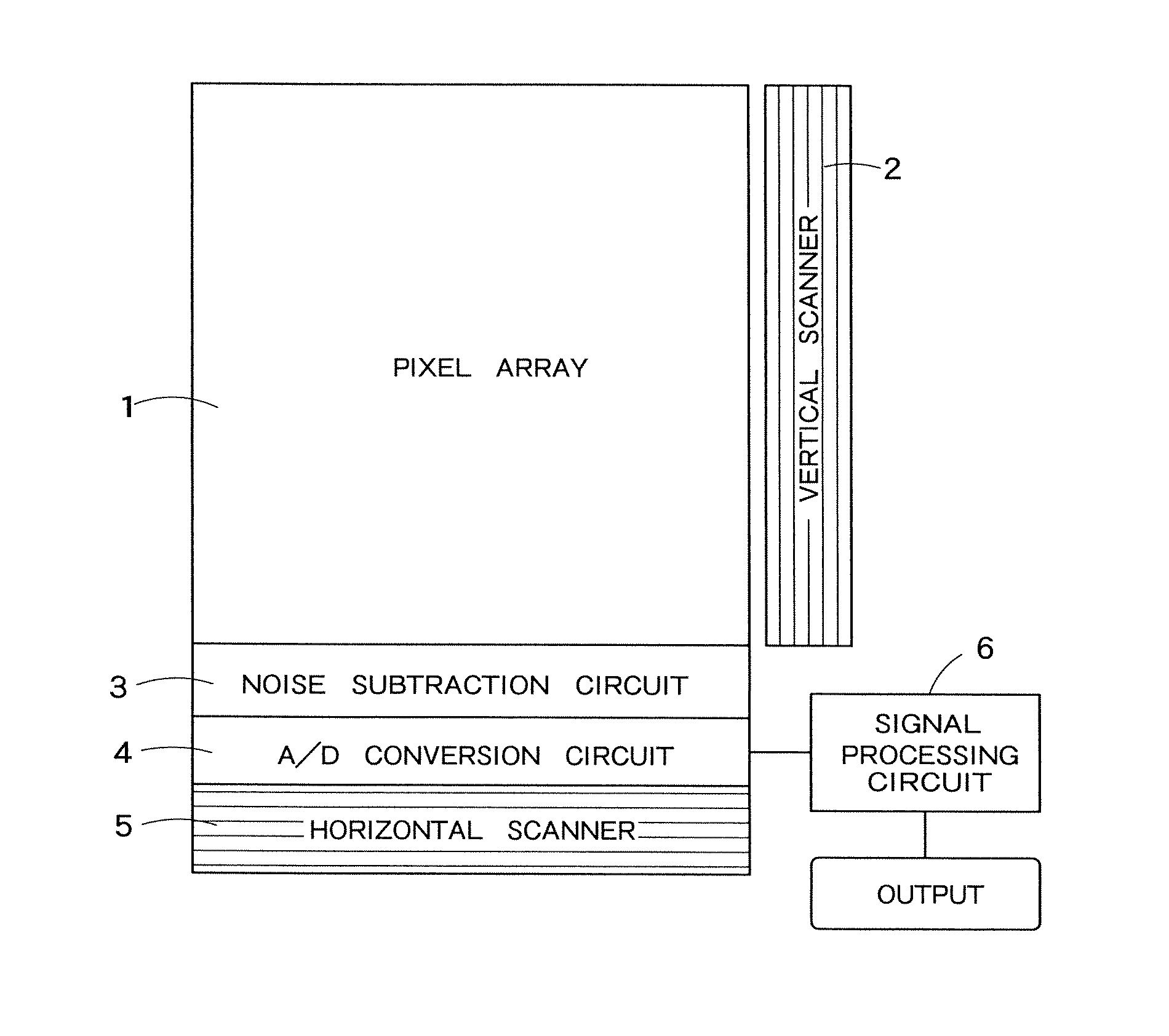
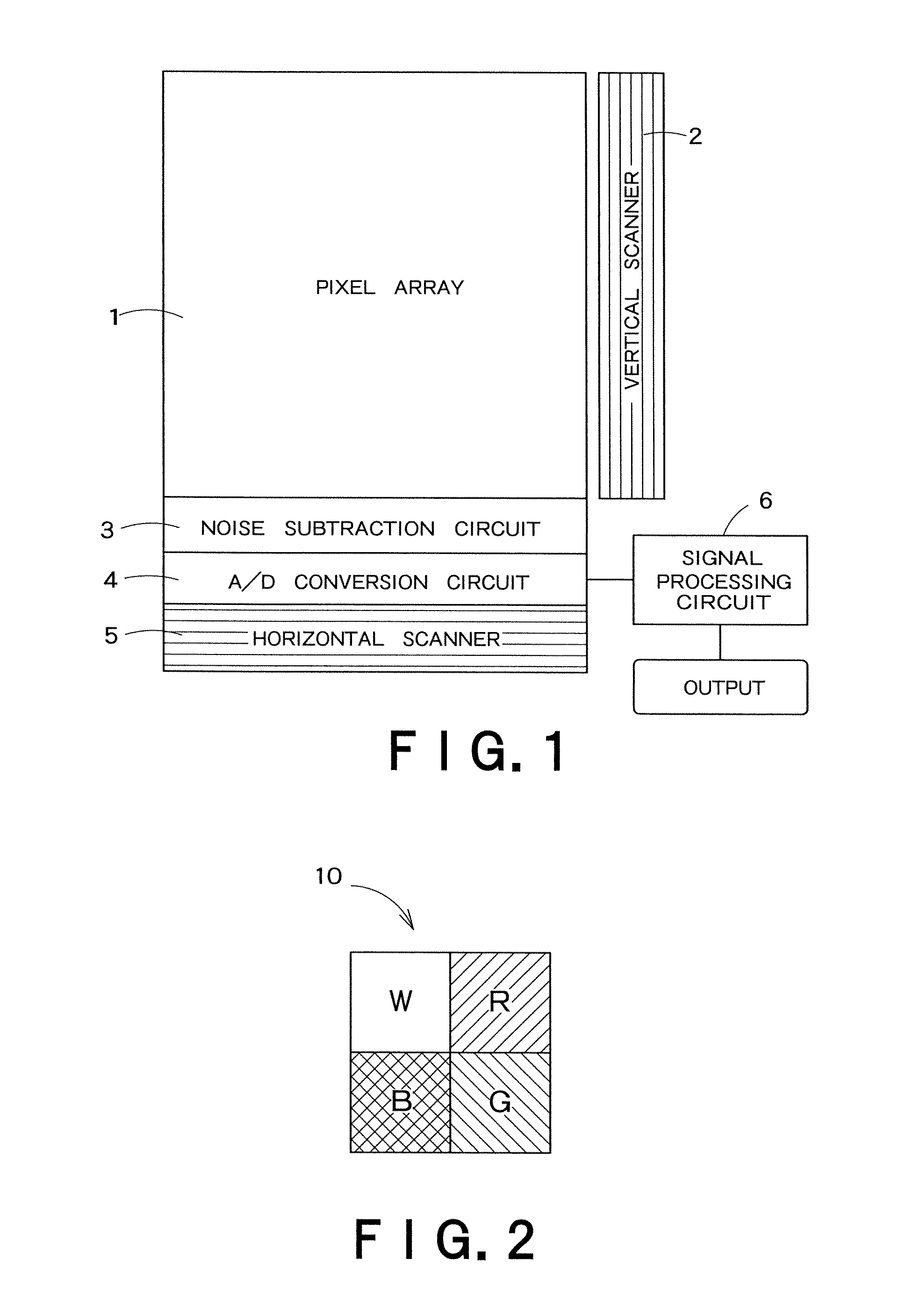
[0094]FIG. 1 is a block diagram showing a schematic configuration of a solid-state image sensor according to an embodiment of the present invention. The solid-state image sensor depicted in FIG. 1 includes a pixel array 1 in which a plurality of pixels each having a photoelectric converting element are arranged in a matrix form, a vertical scanner 2 that sequentially supplies a driving voltage to respective rows in the pixel array 1, a noise subtraction circuit 3 that performs processing to remove noise included in an imaging signal subjected to photoelectric conversion in each pixel, an A / D conversion circuit 4 that performs A / D conversion on the imaging signal output from the noise subtraction circuit 3, a horizontal scanner 5 that sequentially selects and reads A / D-converted imaging data in accordance with each column, and a signal processing circuit 6 that performs later-explained signal processing to the imaging data.

[0095]The signal processing circuit 6 receives imaging data f...

second embodiment

[0121]A second embodiment explained below is characterized in that a white color data value W of a pixel W is color-separated into three pieces of color data R, G, and B.

[0122]Although a solid-state image sensor according to the second embodiment is configured like the embodiment depicted in FIG. 1, the second embodiment is different from the first embodiment in a processing operation of a signal processing circuit 6. A difference from the first embodiment will be mainly explained hereinafter.

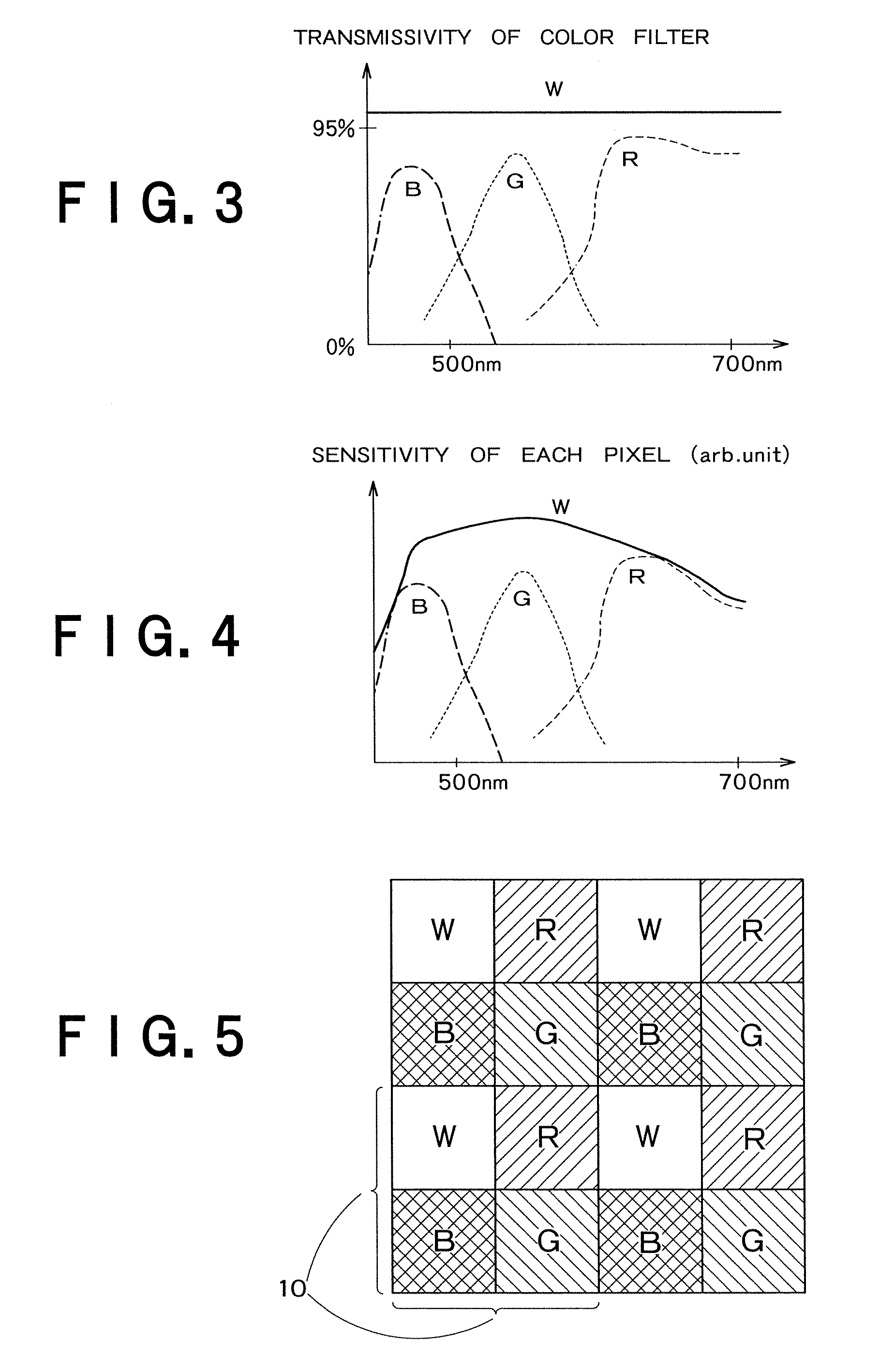
[0123]Even in the second embodiment, a pixel block formed of three rows and three columns with a pixel W being arranged at the center is judged as a basic unit for clearly explaining color separation processing. An actual basic unit of the pixel block is not restricted to a configuration of three rows and three columns.

[0124]FIG. 11 is a block diagram showing an example of an internal configuration of the signal processing circuit 6 according to the second embodiment. The signal processing circ...

third embodiment

[0141]A third embodiment is characterized in that white color data is used at a low illuminance to perform restoration processing of a color signal.

[0142]Although a solid-state image sensor according to the third embodiment has the same configuration as that depicted in FIG. 1, the third embodiment is different from the first and the second embodiments in a processing operation of a signal processing circuit 6. Differences from the first and the second embodiments will be mainly explained hereinafter.

[0143]In the third embodiment, a pixel block formed of three rows and three columns with a pixel W being placed at the center is likewise judged as a basic unit in order to facilitating understanding color separation processing, and an actual basic unit of the pixel block is not restricted to a structure formed of three rows and three columns.

[0144]FIG. 17 is a block diagram showing an example of an internal configuration of a signal processing circuit 6 according to the third embodimen...


PUM


Abstract

A solid-state image sensor has a plurality of pixels, a read-out circuit and a signal processing section. The plurality of pixels includes a plurality of first pixels, a plurality of second pixels, a plurality of third pixels and a plurality of fourth pixels. The signal processing section includes a color acquisition section, a first judgment section configured to determine whether or not the white data value W in the target pixel block is smaller than a predetermined first set value, and a white color correction section configured to perform correction processing of the white color data value W in the target pixel block based on the following Expression (1) when the judgment result of the first judgment section is NO, and to output the white data value W by itself without performing the correction processing based on the Expression (1) when the judgment result of the first determination section is YES;W′=S1C1+S2C2+S3C3  (1)where each of S1, S2, and S3 is a coefficient that is determined based on a color balance.

Description

CROSS REFERENCE TO RELATED APPLICATIONS[0001]This application is based upon and claims the benefit of priority from the prior Japanese Patent Application No. 2006-165053, filed on Jun. 14, 2006 and Japanese Patent Application No. 2007-16971, filed on Jan. 26, 2007, the entire contents of which are incorporated herein by reference.BACKGROUND OF THE INVENTION[0002]1. Field of the Invention[0003]The present invention relates to a solid-state image sensor in which a plurality of pixels each having a photoelectric converting element are arranged in a matrix form.[0004]2. Related Art[0005]In recent years, MOS (CMOS) image sensors have been actively developed. In particular, with miniaturization (a reduction in design rules) of a semiconductor process, single-plate color image sensors each having 5 million or more pixels at a pixel pitch of, e.g., 2.5 μm have been commercialized.[0006]This type of MOS image sensor generally includes a color filter having a Bayer arrangement where one red (...

Claims


Application Information

Patent Timeline
Patent Type & Authority Patents(United States)
IPC IPC(8): H04N3/14H04N5/335H04N9/73H04N9/04G06K9/00H04N5/341H04N5/357H04N5/369H04N5/374H04N5/3745H04N9/07
CPCH01L27/14645H04N9/045H04N9/735H01L27/14603H01L27/14621H01L27/14623H01L27/14627H04N2209/046H04N25/133H04N25/135H04N23/843H04N23/88H04N25/76
Inventor HONDA, HIROTOIIDA, YOSHINORIEGAWA, YOSHITAKAITOH, GOH
Owner KK TOSHIBA
Why Eureka
Try Eureka