Driving circuit including shift register and flat panel display device using the same

a technology of shift register and display device, which is applied in the direction of static indicating device, instruments, mechanical equipment, etc., can solve the problems of high driving voltage with increasing display area, deterioration of a-si tft, and heavy weight, so as to improve color reproducibility, improve display quality, and improve contrast ratio

Active Publication Date: 2009-05-05
LG DISPLAY CO LTD
View PDF8 Cites 62 Cited by
  • Summary
  • Abstract
  • Description
  • Claims
  • Application Information

AI Technical Summary

Benefits of technology

[0018]A field sequential mode liquid crystal display device having an improved contrast ratio and an improved color reproducibility, and a driving method thereof is presented. The field sequential mode liquid crystal display device has an improved display quality at a relatively low temperature.

Problems solved by technology

However, the CRTs have some disadvantages, for example, heavy weight, large volume and high driving voltage with increasing display area.
When the plurality of shift registers include an amorphous silicon (a-Si) TFT, the a-Si TFT may be deteriorated due to a high direct current (DC) bias for a long time period.
The non-uniformity in threshold voltage reduces reliability of TFTs.

Method used


Image

  • Driving circuit including shift register and flat panel display device using the same
  • Driving circuit including shift register and flat panel display device using the same
  • Driving circuit including shift register and flat panel display device using the same

Examples


Embodiment Construction

[0037]Reference will now be made in detail to the preferred embodiments of the present invention, an example of which is illustrated in the accompanying drawings.

[0038]To improve the reliability of a shift register including one pull-down unit, a shift register including two pull-down units is suggested, where the variation in characteristics of TFTs such as the threshold voltage shift is be reduced.

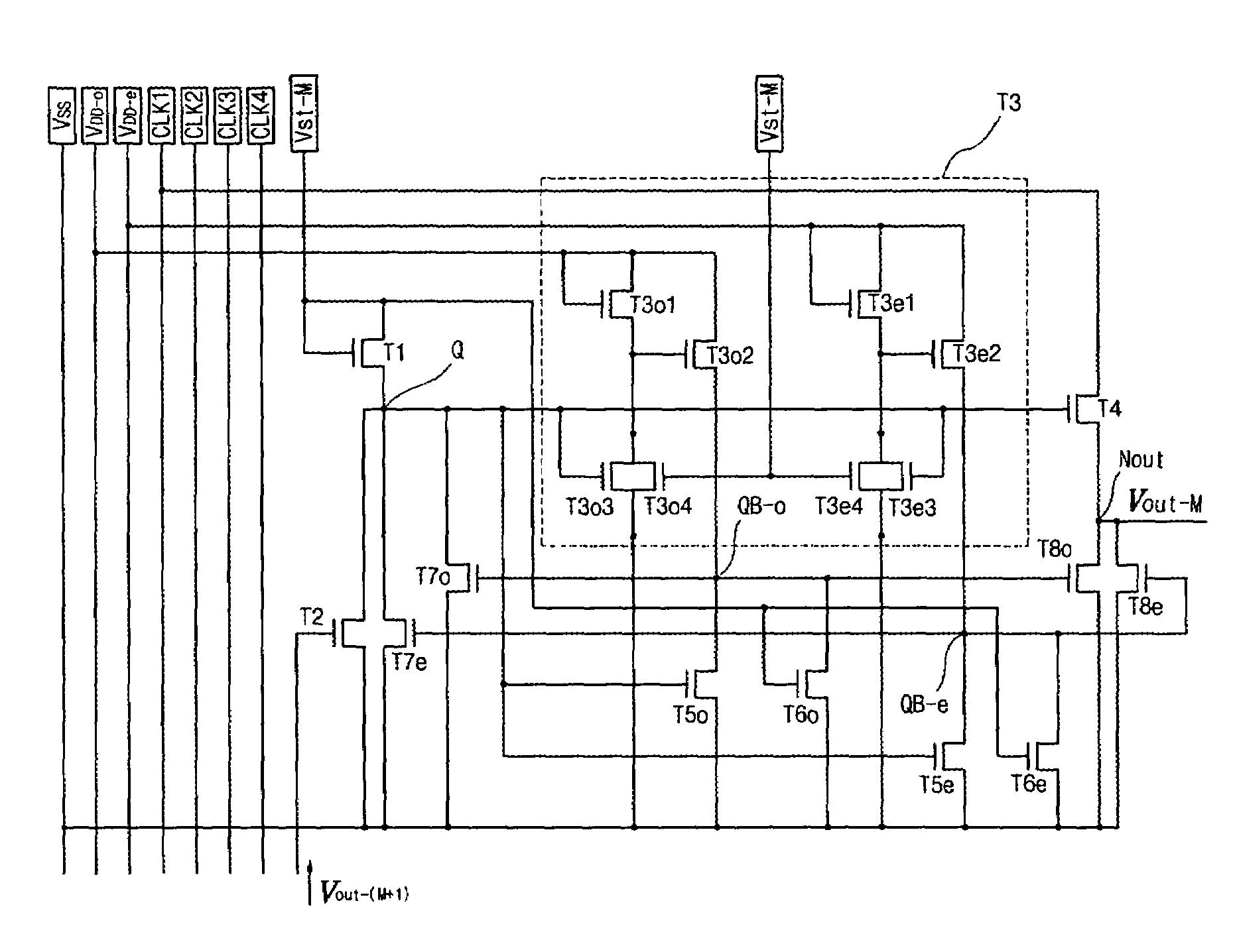
[0039]FIG. 6 is a schematic circuit diagram showing an Nth stage of a shift register including two pull-down units for a liquid crystal display device according to an embodiment of the present invention and FIG. 7 is a schematic timing chart showing signals for driving a shift register of FIG. 6.

[0040]In FIGS. 6 and 7, an Nth stage of a shift register includes a first thin film transistor (TFT) “T1,” a second TFT “T2,” a third odd TFT “T3o,” a third even TFT “T3e,” a fourth odd TFT “T4o,” a fourth even TFT “T4e,” a fifth odd TFT “T5o,” a fifth even TFT “T5e,” a sixth TFT “T6,” a seventh ...


PUM


Abstract

A driving circuit for a flat panel display device includes shift register stages, each containing: a first TFT charging a Q node according to a start signal; a second TFT discharging the Q node according to an output voltage of a next shift register stage; a pull-up unit increasing an output voltage according to the Q node voltage; an odd pull-down unit decreasing the output voltage in an odd frame according to a QB-o node voltage; and an even pull-down unit decreasing the output voltage in an even frame according to a QB-e node voltage. A gate and drain of a third odd TFT connected to the QB-o node are connected to each other and receive an odd source voltage. A gate and drain of the third even TFT connected to the QB-e node are connected to each other and receive an even source voltage.

Description

PRIORITY CLAIM[0001]The present invention claims the benefit of Korean Patent Application No. 2004-0113684, filed in Korea on Dec. 28, 2004, which is hereby incorporated by reference.FIELD OF THE INVENTION[0002]The present invention relates to a driving circuit for a flat panel display device, and more particularly, to a driving circuit having a shift register and a flat panel display device using the same.DISCUSSION OF THE RELATED ART[0003]Cathode ray tubes (CRTs) have been widely used for display devices such as a television and a monitor. However, the CRTs have some disadvantages, for example, heavy weight, large volume and high driving voltage with increasing display area. Accordingly, flat panel display (FPD) devices, such as liquid crystal display (LCD) devices, plasma display panel (PDP) devices and organic electroluminescent display (ELD) devices, having excellent characteristics of light weight and low power consumption have been the subject of recent research.[0004]In gene...

Claims


Application Information

Patent Timeline
Patent Type & Authority Patents(United States)
IPC IPC(8): G09G3/36
CPCG11C19/00G11C19/28F16D65/183F16D55/226F16D2121/04F16D2125/06F16D2125/08
Inventor YOON, SOO-YOUNGJANG, YONG-HOKIM, BINNMOON, SOO-HWAN
Owner LG DISPLAY CO LTD
Why Eureka
Try Eureka