
Semiconductor manufacturing equipment with an open-topped cassette apparatus

a manufacturing equipment and cassette technology, applied in the direction of electric devices, conveyor parts, transportation and packaging, etc., can solve the problems of low strength, inconvenient transportation, inconvenient processing of wafers, etc., and achieve the effect of processing wafers quickly and stably

Active Publication Date: 2011-08-09
MITSUBISHI ELECTRIC CORP
View PDF18 Cites 0 Cited by
  • Summary
  • Abstract
  • Description
  • Claims
  • Application Information

AI Technical Summary

Benefits of technology

[0015]The present invention aims at solving the above-mentioned problems and has for its object to obtain a semiconductor manufacturing apparatus and a semiconductor manufacturing method that are capable of easily and stably processing a wafer irrespective of thickness.
[0018]With the semiconductor manufacturing apparatus and the semiconductor manufacturing method according to the present invention, a wafer can be processed easily and stably irrespective of thickness.

Problems solved by technology

In a semiconductor substrate whose aperture is relatively as large as not less than 6 inches and whose thickness is relatively as thin as not more than 100 μm, its own low strength and bowing or fluxure most probably damage the semiconductor substrate in a semiconductor manufacturing apparatus or during transportation between semiconductor manufacturing apparatuses.
If the width of the groove is too large, there may arise, for example, the problem that a wafer inclines and contacts with the adjacent wafer especially when the wafer is processed in a vertical position within a horizontal diffusion furnace.
Since the foregoing treatments have been performed in the conventional semiconductor manufacturing apparatus, thin wafers and the like that are low in strength have the problem that they might be damaged or deformed during transportation.
Further, when using a plurality of wafers having different thicknesses, there has been the problem that a different processing may become a necessity in a jig or the like depending on the thickness of a wafer, thus complicating the treatment.
However, because the wafer carrier disclosed in Patent document 1 is shaped like a case, there has been the problem that the encasement and takeout of a wafer or the like requires the operations of opening and closing a cover of the wafer carrier, thus complicating the operation.
Also in the wafer protection case disclosed in Patent document 2, there has been the problem that the encasement and takeout of a wafer or the like requires the operations of opening and closing or the like, thus complicating the operation.

Method used


Image

  • Semiconductor manufacturing equipment with an open-topped cassette apparatus
  • Semiconductor manufacturing equipment with an open-topped cassette apparatus
  • Semiconductor manufacturing equipment with an open-topped cassette apparatus

Examples


Embodiment Construction

1. First Preferred Embodiment

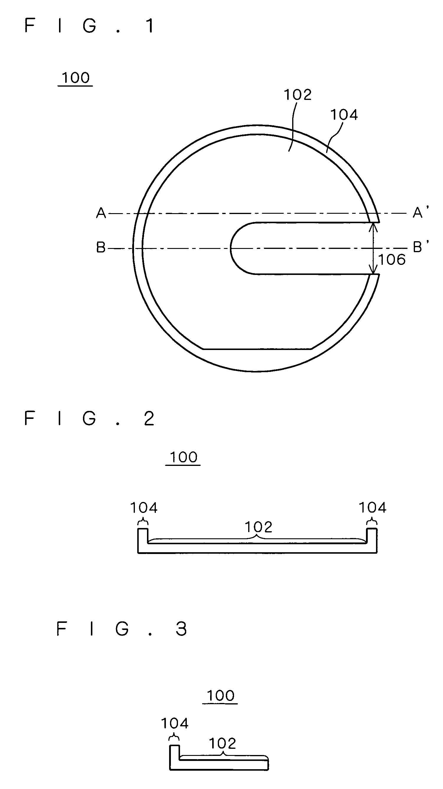
[0067]FIG. 1 is a top view showing a wafer cassette 100 for use in a semiconductor manufacturing apparatus and a semiconductor manufacturing method according to a first preferred embodiment of the present invention. FIG. 2 is a sectional view taken along the line A-A′ in FIG. 1. FIG. 3 is a sectional view taking along the line B-B′ in FIG. 1.

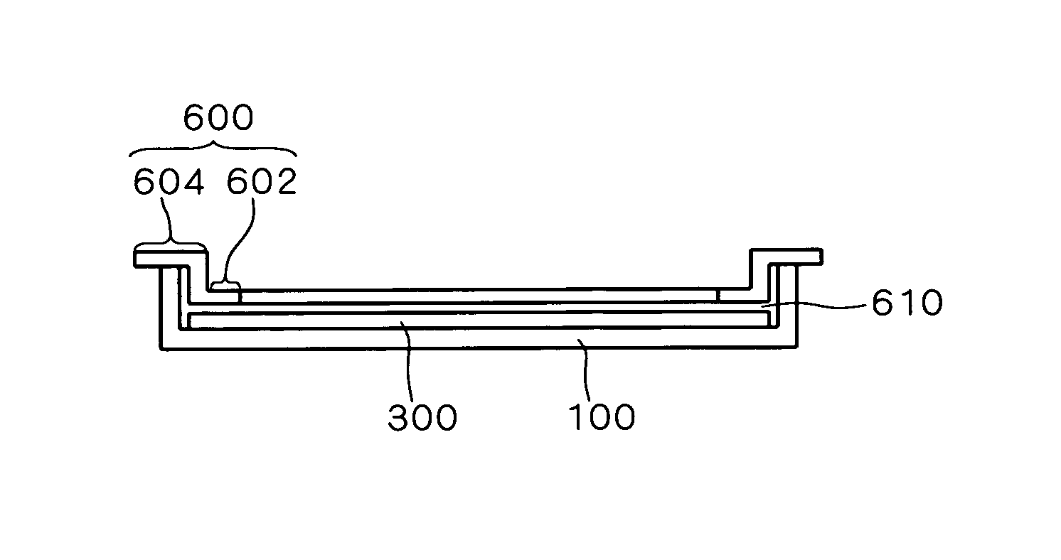
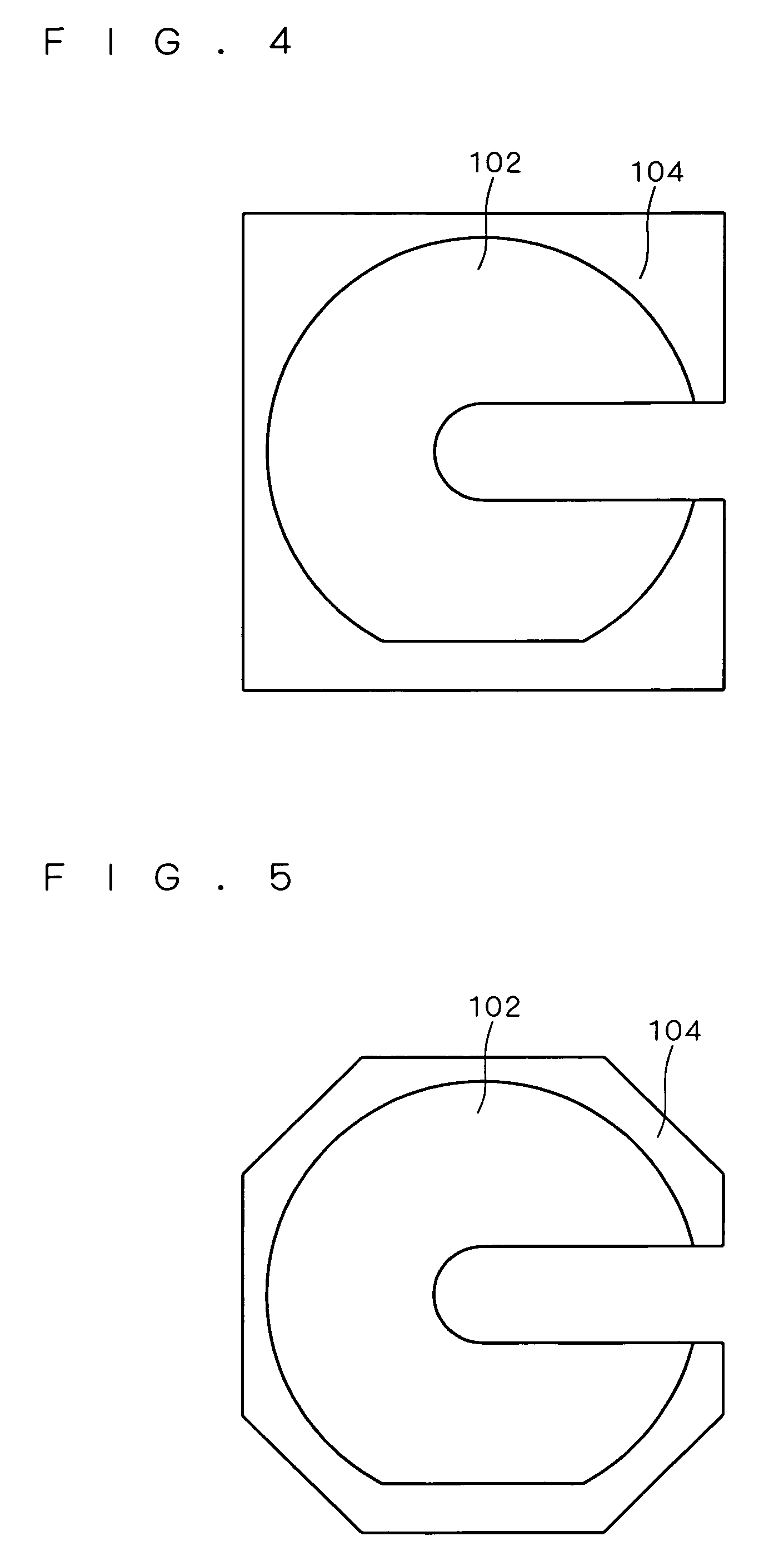
[0068]As shown in FIG. 1, the wafer cassette 100 includes a wafer holding part 102 (a first holding part) for holding a wafer, which is brought into contact with the bottom surface (the underside) of a wafer (a semiconductor substrate) composed of a semiconductor, and a wafer holding part 104 (a second holding part) for holding a wafer, which is brought into contact with a side surface of a wafer. A slotted opening part 106 is disposed from part of the periphery of the wafer holding part 104 to a center section of the wafer holding part 102. As shown in FIGS. 2 and 3, the wafer holding part 102 has a periphery of app...


PUM


Abstract

A semiconductor manufacturing apparatus and a semiconductor manufacturing method, and has as one object to process a wafer easily and stably irrespective of thickness. To achieve the above object, a semiconductor manufacturing apparatus includes: an open-topped cassette that encases a semiconductor substrate; a plurality of processors for performing a predetermined processing of the semiconductor substrate; and a transporting mechanism that transports the cassette encasing the semiconductor substrate between the plurality of processors.

Description

TECHNICAL FIELD[0001]The present invention relates to a semiconductor manufacturing apparatus and a semiconductor manufacturing method, and more particularly to a processing of a semiconductor substrate.BACKGROUND ART[0002]In a conventional vertical semiconductor device in which current is allowed to flow across a first main surface and a second main surface of a semiconductor substrate (semiconductor wafer), the semiconductor substrate has become increasingly more thinned film with the purpose of characteristic improvement (for example, on voltage reduction). On the other hand, in the field of high breakdown voltage semiconductor devices that control high voltages exceeding 1000V, it is necessary to become more thickened film according to breakdown voltage. That is, a semiconductor manufacturing apparatus will be increasingly required to process a plurality of semiconductor substrates having different thicknesses. In a wafer for ULSI, such as DRAM, the tendency to increase aperture...

Claims


Application Information

Patent Timeline
Patent Type & Authority Patents(United States)
IPC IPC(8): H01L21/461
CPCH01L21/67309H01L21/67346H01L21/67778H01L21/223
Inventor TOKUDA, NORIFUMI
Owner MITSUBISHI ELECTRIC CORP
Learn More