System and method for evaluating high frequency time domain in embedded device probing

a high frequency time domain and embedded device technology, applied in the direction of measurement devices, noise figures or signal-to-noise ratio measurement, instruments, etc., can solve the problems of difficult or impossible to pick up test signals at the points of interest by direct manual probing, degradation along each signal trace may significantly affect electrical signal fidelity, and the inaccurate results of such direct manual probing cannot be easily overcome. , to achieve the effect of eliminating the effect of signal degradation

Inactive Publication Date: 2011-08-16
INT BUSINESS MASCH CORP
View PDF3 Cites 2 Cited by
  • Summary
  • Abstract
  • Description
  • Claims
  • Application Information

AI Technical Summary

Benefits of technology

[0005]deriving an inverse transfer function (iG) for the signal path, such that the inverse transfer function (iG) eliminates signal degradation effects from the remote signal (SFE), wherein signal degradation effects are caused by transferring the high-frequency signal (SNE) through the signal path; and
[0010]deriving an inverse transfer function (iG) for the signal path, such that the inverse transfer function (iG) eliminates signal degradation effects from the remote signal (SFE), wherein signal degradation effects are caused by transferring the high-frequency signal (SNE) through the signal path; and
[0015]deriving an inverse transfer function (iG) for the signal path, such that the inverse transfer function (iG) eliminates signal degradation effects from the remote signal (SFE), wherein signal degradation effects are caused by transferring the high-frequency signal (SNE) through the signal path; and

Problems solved by technology

Conventional test probes employing a direct measurement of signals at points of interest have difficulties in testing modern electrical machines embedding multiple physical devices, because sizes of the embedded physical devices become smaller and higher frequency signal bandwidths are required for increased speed properties of smaller embedded physical devices.
It is difficult or impossible to pick up test signals at the points of interest by direct manual probing.
Even when an embedded device can be operated in a probing environment, because signal traces between conventional test probes and the embedded device are typically needed to transfer stimulating and resulting signals, degradation along each signal trace may significantly impact electrical signal fidelity.
The difficulties in direct manual probing and inaccurate results of such direct manual probing cannot be easily overcome by adjusting physical characteristics of the probing environment.

Method used


Image

  • System and method for evaluating high frequency time domain in embedded device probing
  • System and method for evaluating high frequency time domain in embedded device probing
  • System and method for evaluating high frequency time domain in embedded device probing

Examples


Embodiment Construction

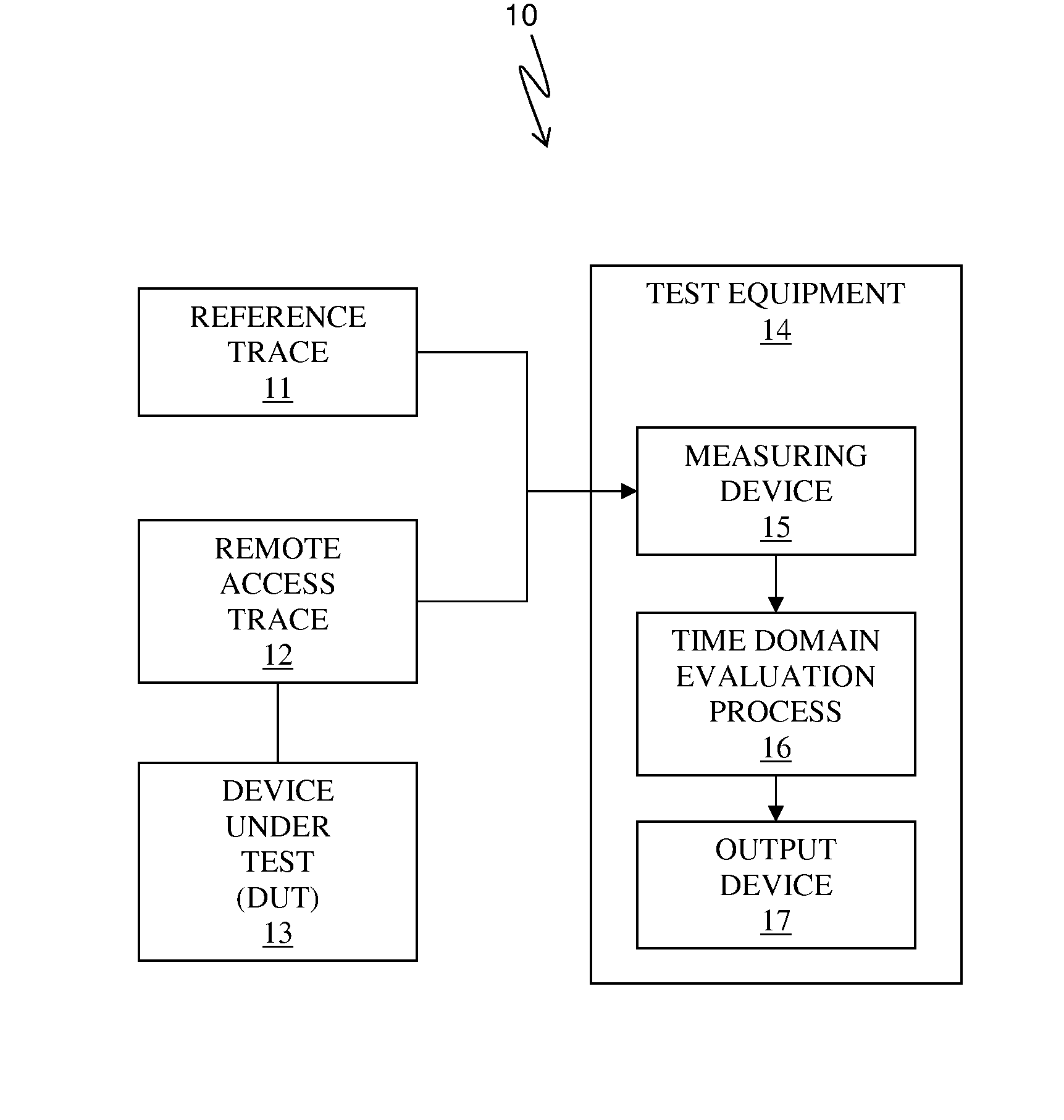
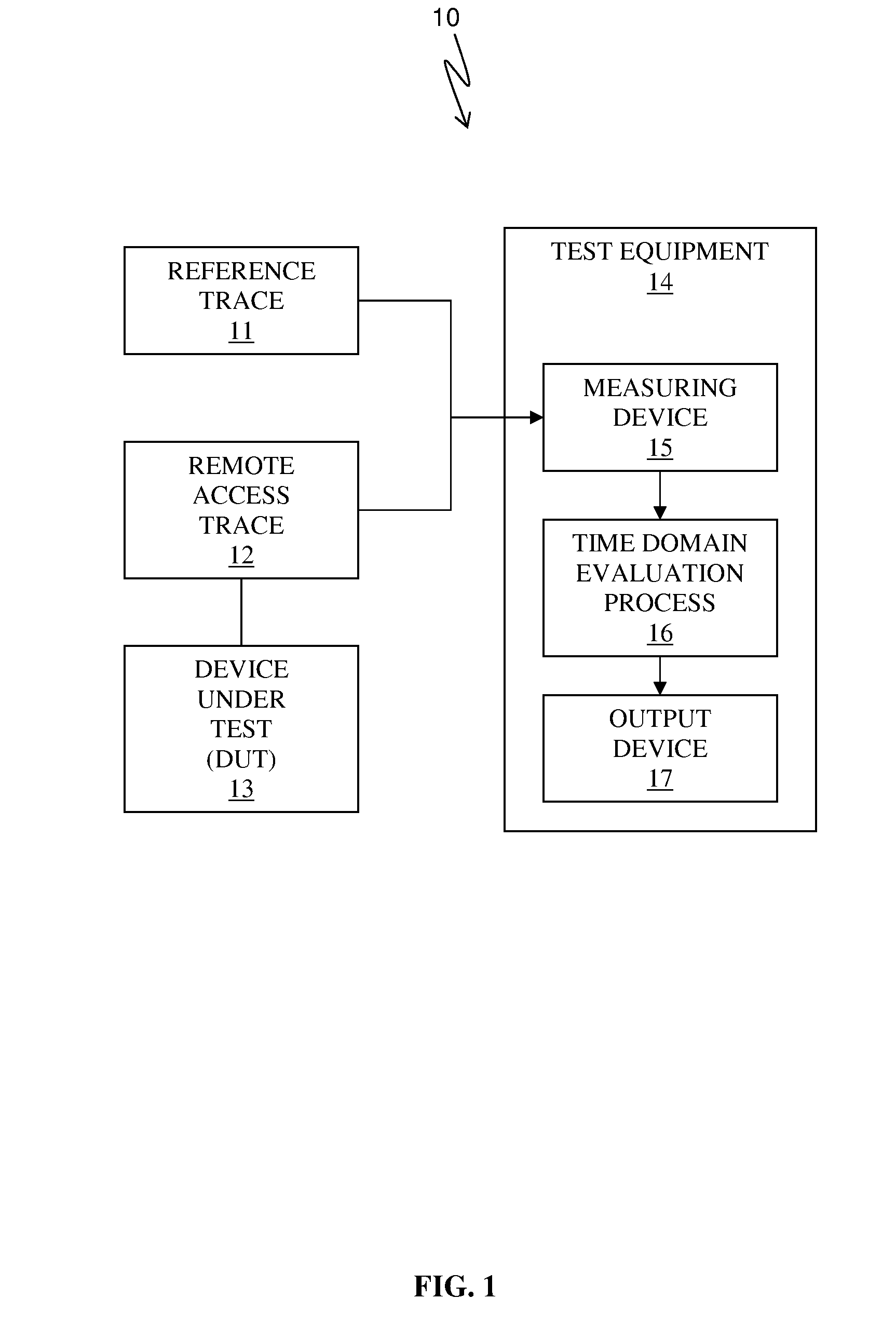
[0028]FIG. 1 illustrates a test probe system 10 for evaluating time domain signal data in an electrical device, in accordance with embodiments of the present invention. The test probe system 10 comprises a reference trace 11, a remote access trace 12, a device under test (DUT) 13, and a test equipment 14.

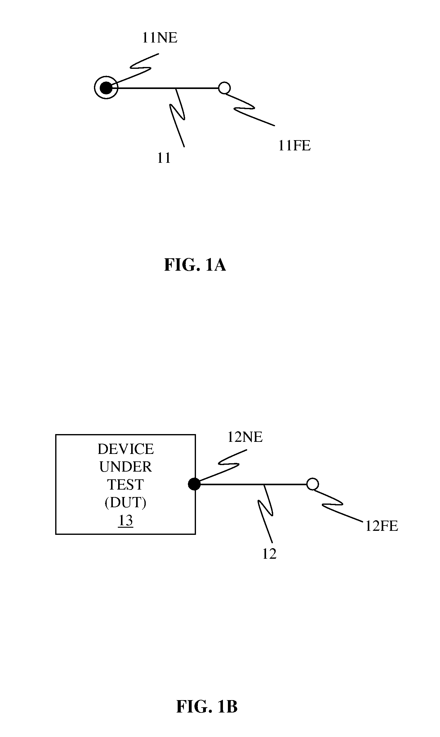
[0029]The reference trace 11 is an electrical signal path that is used to characterize and to simulate electrical properties of the remote access trace 12. See FIG. 1A, infra, for details of the reference trace 11.

[0030]The remote access trace 12 is another electrical signal path that is used to probe a high-frequency electrical signal at a point of interest on the device under test (DUT) 13, which has physical dimension and electrical properties that are equivalent to the reference trace 11. In this specification, the high-frequency electrical signal is any electrical signal of frequencies typically above 1 GHz. See FIG. 1B, infra, for details of the remote access trace 12.

[0031]Th...


PUM


Abstract

A system and associated method for evaluating a high-frequency signal at a point of interest on a signal path from a remote signal at a remote pickup point on the signal path. The point of interest is located on a device under test that is coupled to test equipment via the signal path. The high-frequency signal at the point of interest is calculated from the remote signal at the remote pickup point with an inverse transfer function that eliminates degradation effects on the high-frequency signal that is transferred through the signal path. The inverse transfer function may be calculated from measurements acquired in a test signal transfer through a reference path that simulates electrical properties of the signal path, or configured to a predetermined function if electrical properties of the signal path are known.

Description

FIELD OF THE INVENTION[0001]The present invention discloses a system and associated method for improved probing of electrical signals and accurate measurements thereof.BACKGROUND OF THE INVENTION[0002]Conventional test probes employing a direct measurement of signals at points of interest have difficulties in testing modern electrical machines embedding multiple physical devices, because sizes of the embedded physical devices become smaller and higher frequency signal bandwidths are required for increased speed properties of smaller embedded physical devices. It is difficult or impossible to pick up test signals at the points of interest by direct manual probing. Even when an embedded device can be operated in a probing environment, because signal traces between conventional test probes and the embedded device are typically needed to transfer stimulating and resulting signals, degradation along each signal trace may significantly impact electrical signal fidelity. The difficulties i...

Claims


Application Information

Patent Timeline
Patent Type & Authority Patents(United States)
IPC IPC(8): G06F19/00
CPCG01R31/2837G01R1/06766G01R1/06772
Inventor DIEPENBROCK, JOSEPH CURTISFRECH, ROLAND
Owner INT BUSINESS MASCH CORP
Why Eureka
Try Eureka