Object-processing apparatus controlling production of particles in electric field or magnetic field

a technology of object processing and electric field, applied in the direction of coating, chemical vapor deposition coating, electric discharge tube, etc., can solve problems such as defects in manufactured electronic devices

Inactive Publication Date: 2011-11-08
RENESAS ELECTRONICS CORP
View PDF10 Cites 236 Cited by
  • Summary
  • Abstract
  • Description
  • Claims
  • Application Information

AI Technical Summary

Problems solved by technology

When the dielectric deposits are peeled from the internal members, many particles are produced in the processing chamber so that the object may be contaminated with the particles, resulting in occurrence of defects in the manufactured electronic devices.

Method used


Image

  • Object-processing apparatus controlling production of particles in electric field or magnetic field
  • Object-processing apparatus controlling production of particles in electric field or magnetic field
  • Object-processing apparatus controlling production of particles in electric field or magnetic field

Examples


first embodiment

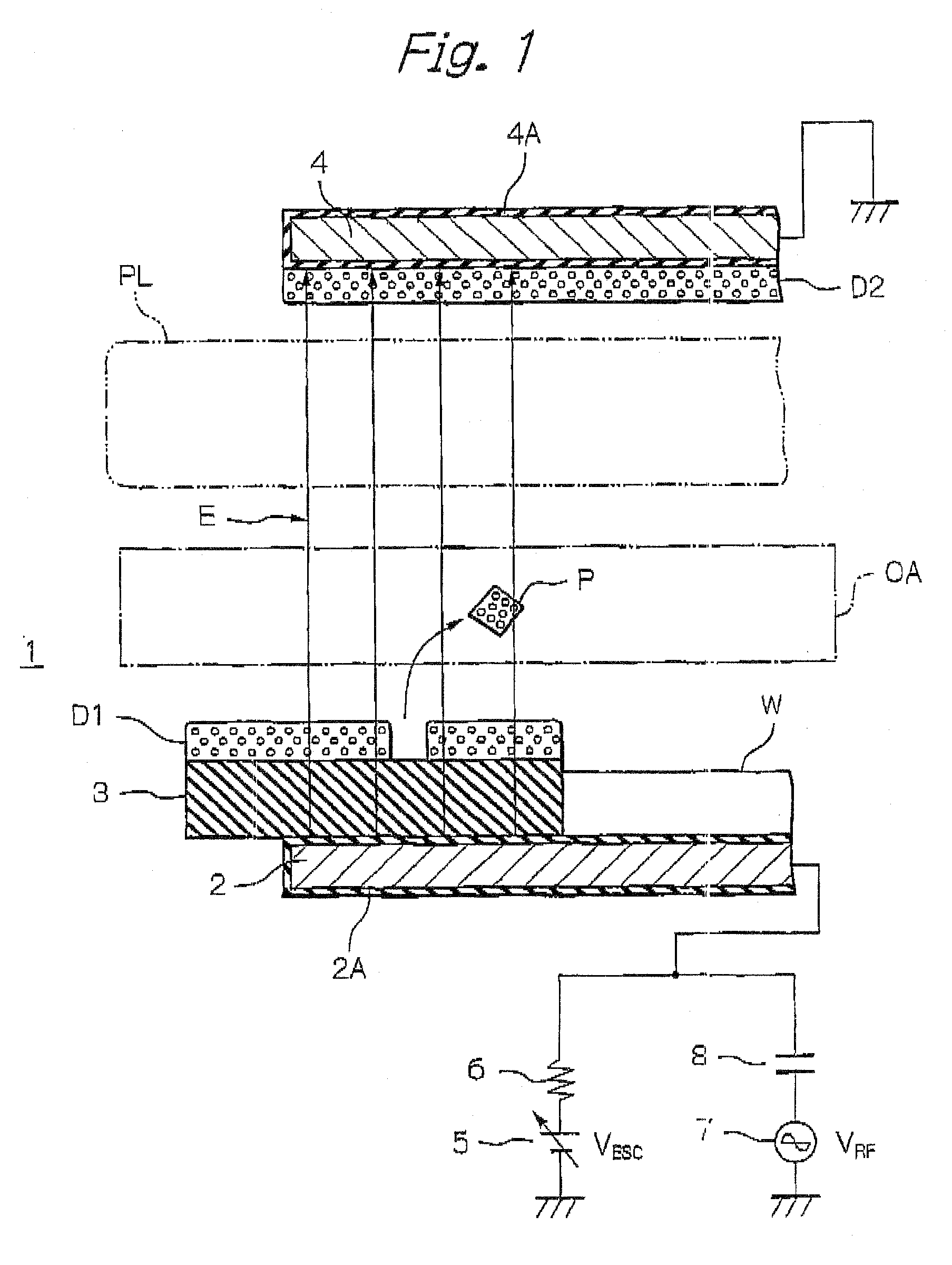
[0081]Firsts with reference to FIG. 3 which is a cross-sectional view of a first embodiment of the apparatus according to the present invention, the first embodiment is constituted as an anode-coupled type plasma CVD apparatus.

[0082]The anode-coupled type plasma CVD apparatus includes a housing 10 having a bottom wall section 10A, a side wall section 10B and a top wall section 10C which define a processing chamber 10D. The housing 10 itself is formed of a suitable metal material such as aluminum or the like, and the inner wall surfaces of the bottom, side aid top wall sections 10A, 10B and 10C of the housing 10 are coated with silicon dioxide (SiO2) so that silicon dioxide layers 10E are formed thereon.

[0083]The housing 10 is provided with exhaust passages 10F formed in the bottom wall section 10A, and the exhaust passages 10F are in communication with a vacuum source not shown) so that a vacuum state is created in the processing chamber 10D.

[0084]Also, the housing 10 is provided wi...

second embodiment

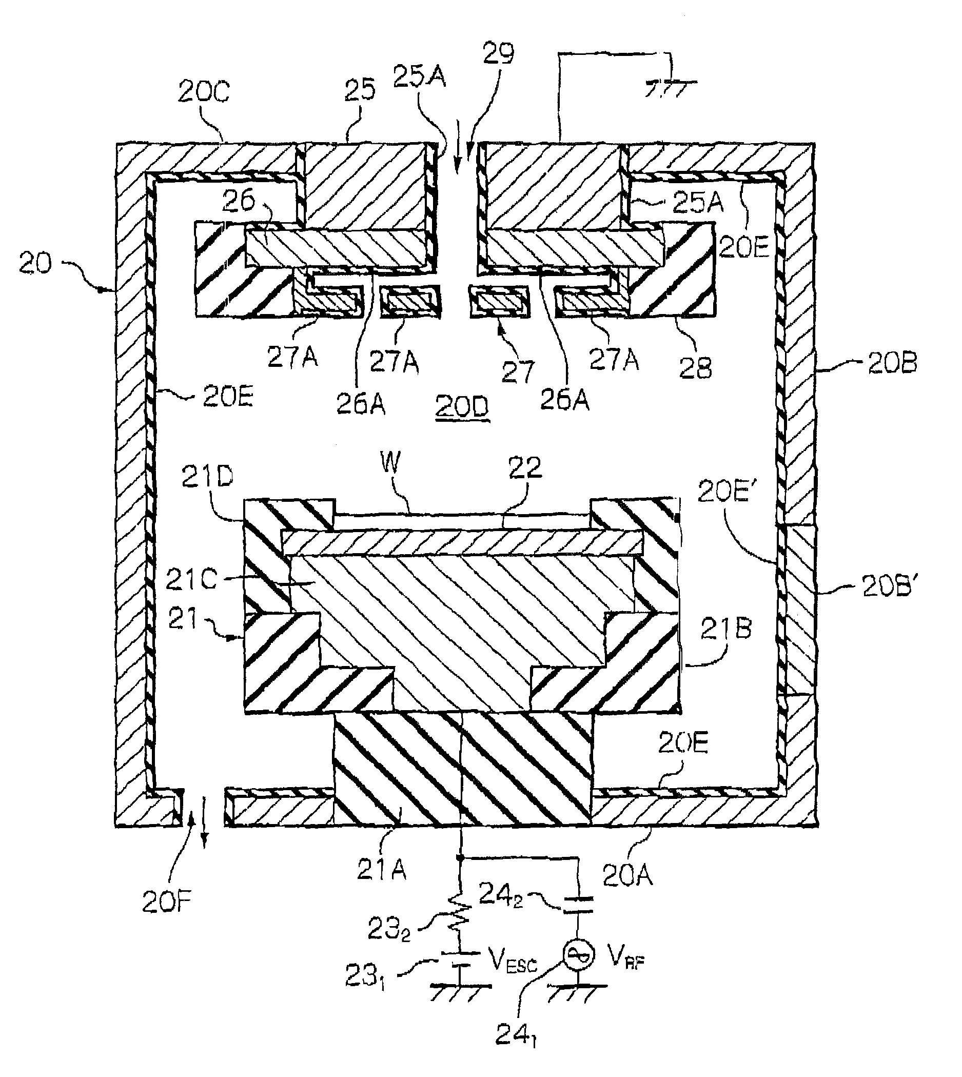
[0100]With reference to FIG. 4 which is a cross-sectional view of a second embodiment of the apparatus according to the present inventions the second embodiment is constituted as a cathode-coupled type plasma etching apparatus.

[0101]The cathode-coupled type plasma etching apparatus includes a housing 20 having a bottom wall section 20A, a side wall section 20B and a top wall section 20C which define a processing chamber 20D. The housing 20 itself is formed of a suitable metal material such as aluminum or the like, and the inner wall surfaces of the bottom, side and top wall sections 20A, 20B and 20C of the housing 20 are coated with a suitable dielectric material such as YAG, barium titanate (BaTiO3), lead zirconate / titanate (Pb(Zr,Ti)O3) or the like, so that dielectric layers 20E are formed thereon.

[0102]The side wall section 20B is provided with a gate valve 20B′ which is openable for introducing an object such as a silicon wafer W to be processed into the processing chamber 20D a...

third embodiment

[0125]With reference to FIG. 5 which is a cross-sectional view of a third embodiment of the apparatus according to the present invention, the third embodiment is also constituted as a cathode-coupled type plasma etching apparatus.

[0126]The cathode-coupled type plasma etching apparatus includes a housing 30 having a bottom wall section 30A, a side wall section 30B and a top wall section 30C which define a processing chamber 30D. The housing 30 itself is formed of a suitable metal material such as aluminum or the like.

[0127]The inner surface of the bottom wall section 30A is coated with a first type dielectric material such as titanium dioxide (TiO2), potassium dihydrogenphosphate (KH2PO4), barium zirconate (PbZrO3) or the like, so that a dielectric layer 30A1 is formed thereon. Also, a lower area of the inner surface of the side wall section 30B is also coated with the aforesaid first type dielectric material such as titanium dioxide (TiO2), potassium dihydrogenphosphate (KH2PO4), ba...


PUM

PropertyMeasurementUnit
self-biased voltageaaaaaaaaaa

Abstract

An apparatus includes a housing defining a chamber in which an electric field is generated, and an internal member provided in the chamber. At least one part of the internal member is formed of a dielectric material. A process is executed in the chamber so that a dielectric deposit is formed on the at least one part of the internal member. An m1(d∈1 / dm1) value of the dielectric material and an m2(d∈2 / dm2) value of the dielectric deposit are set so that production of particles from the deposit is properly controlled. The term m1 is a mass density of the dielectric material, ∈1 is a permittivity of the dielectric material, m2 is a mass density of the dielectric deposit, and ∈2 is a permittivity of the dielectric deposit.

Description

BACKGROUND OF THE INVENTION[0001]1. Field of the Invention[0002]The present invention relates to an apparatus which involves generation of an electric field or a magnetic filed, and more particularly relates to such an apparatus in which manufacture, measurement or examination is carried out in the electric field or the magnetic field so that all object to be manufactured, measured or examined can be protected from being contaminated with particles produced in the apparatus.[0003]2. Description of the Related Art[0004]As a representative apparatus which involves generation of an electric field or a magnetic field, there are a plasma etching apparatus, a chemical vapor deposition (CVD) apparatus, a plasma sputtering apparatus, a focused ion beam (FIB) apparatus, an electron beam (EB) exposure apparatus, an electron microscopic apparatus and so on.[0005]For example, the plasma etching apparatus is used to process an object to manufacture electronic devices. When the electronic devices...

Claims


Application Information

Patent Timeline
Patent Type & Authority Patents(United States)
IPC IPC(8): B05C11/00
CPCC23C16/4404H01J37/09H01J37/16H01J37/32467H01J37/32477H01J2237/022H01J2237/026
Inventor ITAGAKI, YOUSUKEITO, NATSUKOUESUGI, FUMIHIKO
Owner RENESAS ELECTRONICS CORP
Why Eureka
Try Eureka