System and method for running test and redundancy analysis in parallel

a memory device and parallel technology, applied in the field of memory device testing, can solve the problems of slow whole run, time-consuming and relatively expensive tests comprising test patterns, and cell not being usable,

Active Publication Date: 2011-12-27
MICRON TECH INC
View PDF38 Cites 11 Cited by
  • Summary
  • Abstract
  • Description
  • Claims
  • Application Information

AI Technical Summary

Problems solved by technology

In a relatively large array, it can be expected that some cells will not be usable.
For relatively large arrays, these tests comprising test patterns can be time-consuming and relatively expensive.
When the step S970 waits for completion of the step S950, the test as a whole runs slower than the speed at which the ATE can perform the test patterns, which adds time and cost to the DUT.

Method used


Image

  • System and method for running test and redundancy analysis in parallel
  • System and method for running test and redundancy analysis in parallel
  • System and method for running test and redundancy analysis in parallel

Examples


Embodiment Construction

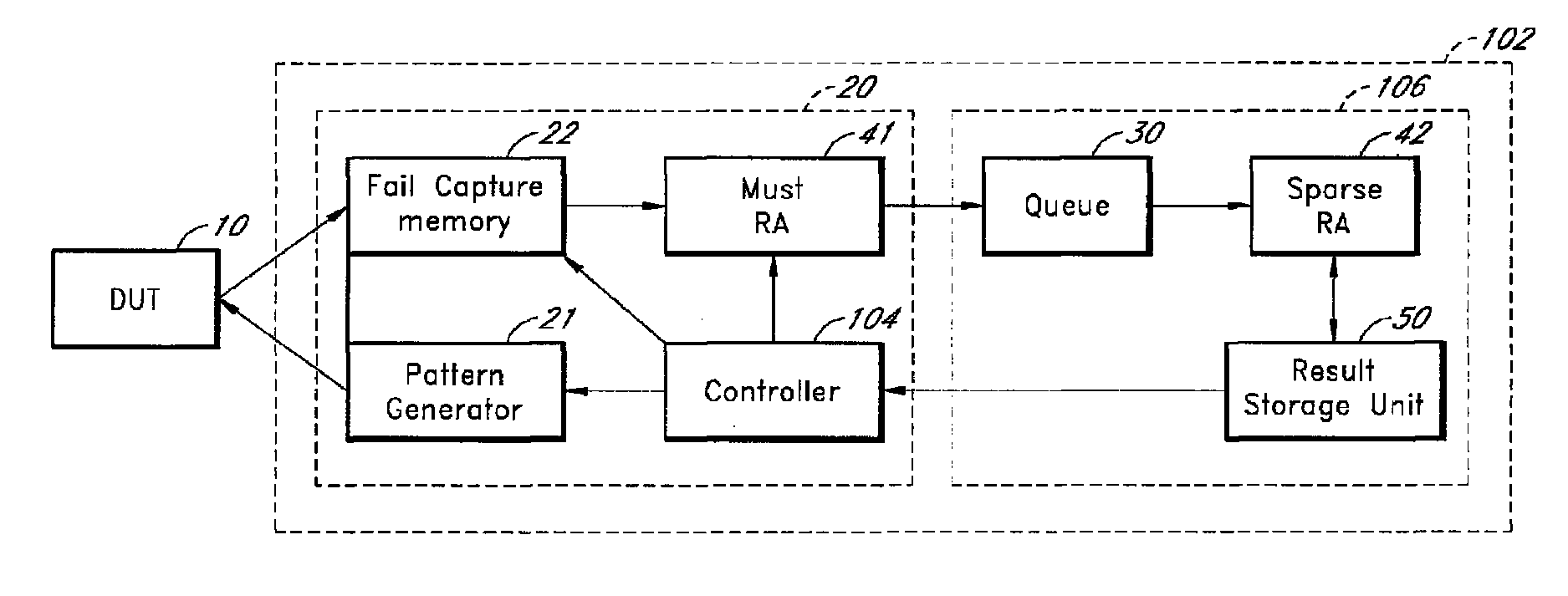
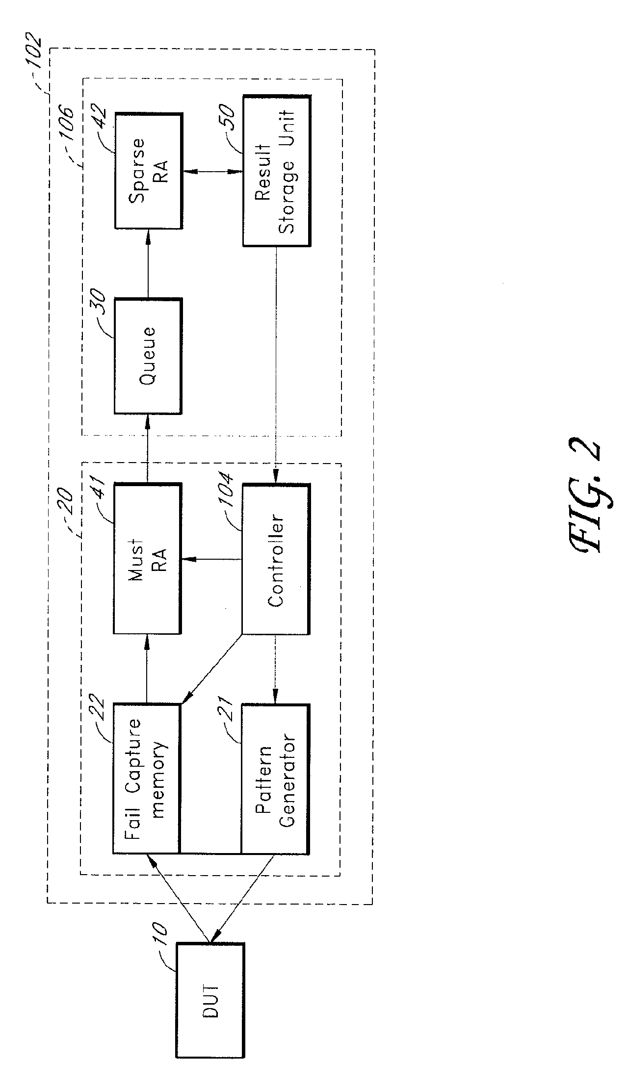
[0015]FIG. 2 shows a schematic block diagram illustrating an apparatus 102 for testing and / or repairing a memory device under test (DUT) 10. The memory device can include any memory device such as DRAM, SDRAM, SRAM, MRAM, FRAM, Flash, EEPROM, PCRAM, etc.

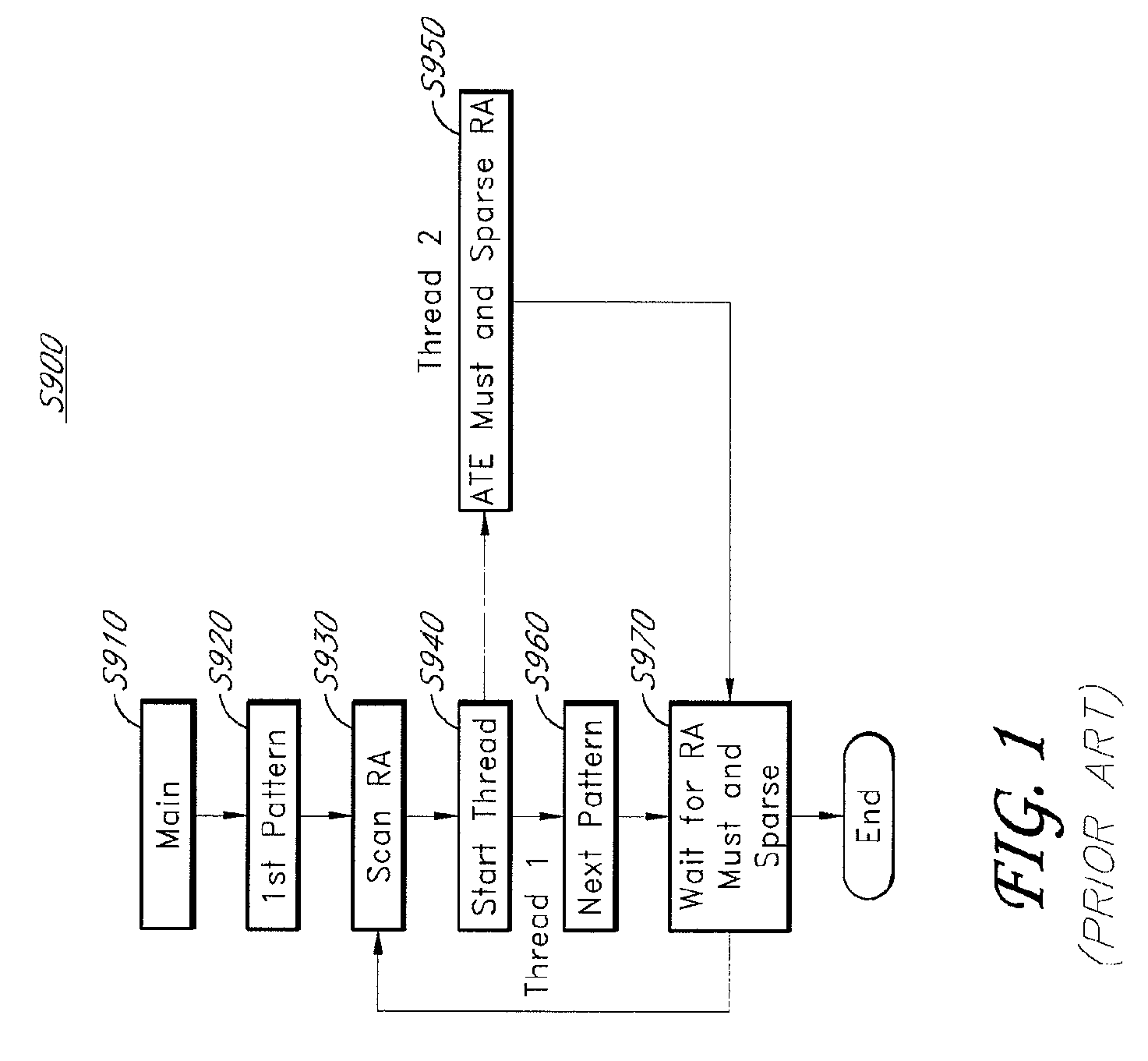
[0016]The apparatus 102 comprises a tester 20, a fail capture memory 22, a must redundancy analyzer 41, a queue 30, a sparse redundancy analyzer 42, a result storage unit 50, a pattern generator 21, and a controller 104. The tester 20 performs tests (test patterns) on the DUT 10 to determine memory locations that fail. The “fails” are collected and stored temporarily at the fail capture memory 22 in the tester 20. The must redundancy analyzer 41 and the sparse redundancy analyzer 42 process the information on the fails to produce a solution to repair the problematic memory locations. The controller 104 is configured to control the pattern generator 21, the fail capture memory 22, and the must redundancy analyzer 41 in the tester 20. ...


PUM


Abstract

A memory redundancy analyzing apparatus having a tester, a queue, and a redundancy analyzer is provided. The tester includes testing portions for different types of fails, and each of the testing portions performs multiple tests on the memory locations and outputs fail information for at least a part of the memory device. The queue stores the fail information. The redundancy analyzer processes the fails using the fail information and produces a plurality of repair solutions. The types of fails include must fails and sparse fails. The fail information is transmitted to the queue, and the fail information includes at least a part of the fail information for the entire memory device. The tester can operate asynchronously from the redundancy analyzer.

Description

CROSS-REFERENCE TO RELATED APPLICATION[0001]This application is a divisional application of U.S. application Ser. No. 11 / 739,599, filed Apr. 24, 2007, the entirety of which is incorporated by reference herein.BACKGROUND[0002]1. Field of the Invention[0003]One embodiment generally relates to test of memory devices. In particular, one embodiment relates to systems and methods of repairing memory devices.[0004]2. Description of the Related Art[0005]Semiconductor memory devices can be found in a wide variety of electronics devices. Modern memory devices are relatively large in size and relatively inexpensive. A memory device typically includes at least one array of memory cells arranged in rows and columns. In a relatively large array, it can be expected that some cells will not be usable. Accordingly, redundant rows and columns exist to repair the defective cells via redundancy analysis. Tests are performed on memory devices to identify the cells that need to be replaced. For relativel...

Claims


Application Information

Patent Timeline
Patent Type & Authority Patents(United States)
IPC IPC(8): G11C29/00
CPCG11C29/56G11C29/56004G11C29/56008G11C29/72
Inventor KOPEL, KRISTOPHER
Owner MICRON TECH INC
Why Eureka
Try Eureka