
Semiconductor device having sealing ring

a technology of sealing ring and semiconductor device, which is applied in the direction of semiconductor device details, semiconductor/solid-state device details, electrical apparatus, etc., can solve the problems of insufficient impact prevention of passivation film, cracks, etc., and achieve the effect of preventing cracks, preventing chipping, and preventing degradation of reliability and moisture resistance of semiconductor devi

Active Publication Date: 2012-04-24
PANASONIC CORP
View PDF9 Cites 3 Cited by
  • Summary
  • Abstract
  • Description
  • Claims
  • Application Information

AI Technical Summary

Benefits of technology

"The invention relates to a semiconductor device that prevents chippings, cracks, and other damage from spreading into the chip region during the dicing process. The invention includes an interlayer insulating film, a winding, a seal ring, and a protective film. The protective film is separated from the seal ring and has an opening. The opening allows the interlayer insulating film to be exposed and prevents impact from spreading into the chip region. The invention prevents degradation of reliability and moisture resistance of the semiconductor device."

Problems solved by technology

Therefore, the passivation film cannot sufficiently prevent impact, cracks, and the like from spreading from the outside toward the inside of the chip region.

Method used


Image

  • Semiconductor device having sealing ring
  • Semiconductor device having sealing ring
  • Semiconductor device having sealing ring

Examples


first embodiment

[0078](First Embodiment)

[0079]Hereinafter, a semiconductor device and a manufacturing method thereof according to a first embodiment of the invention will be described with reference to the figures.

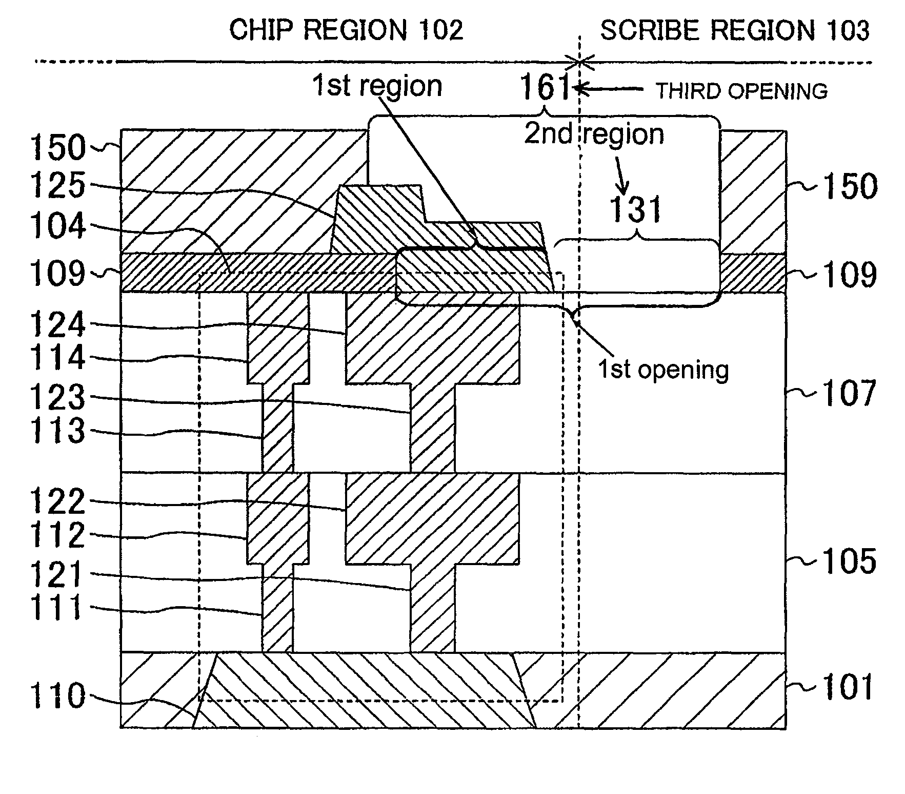
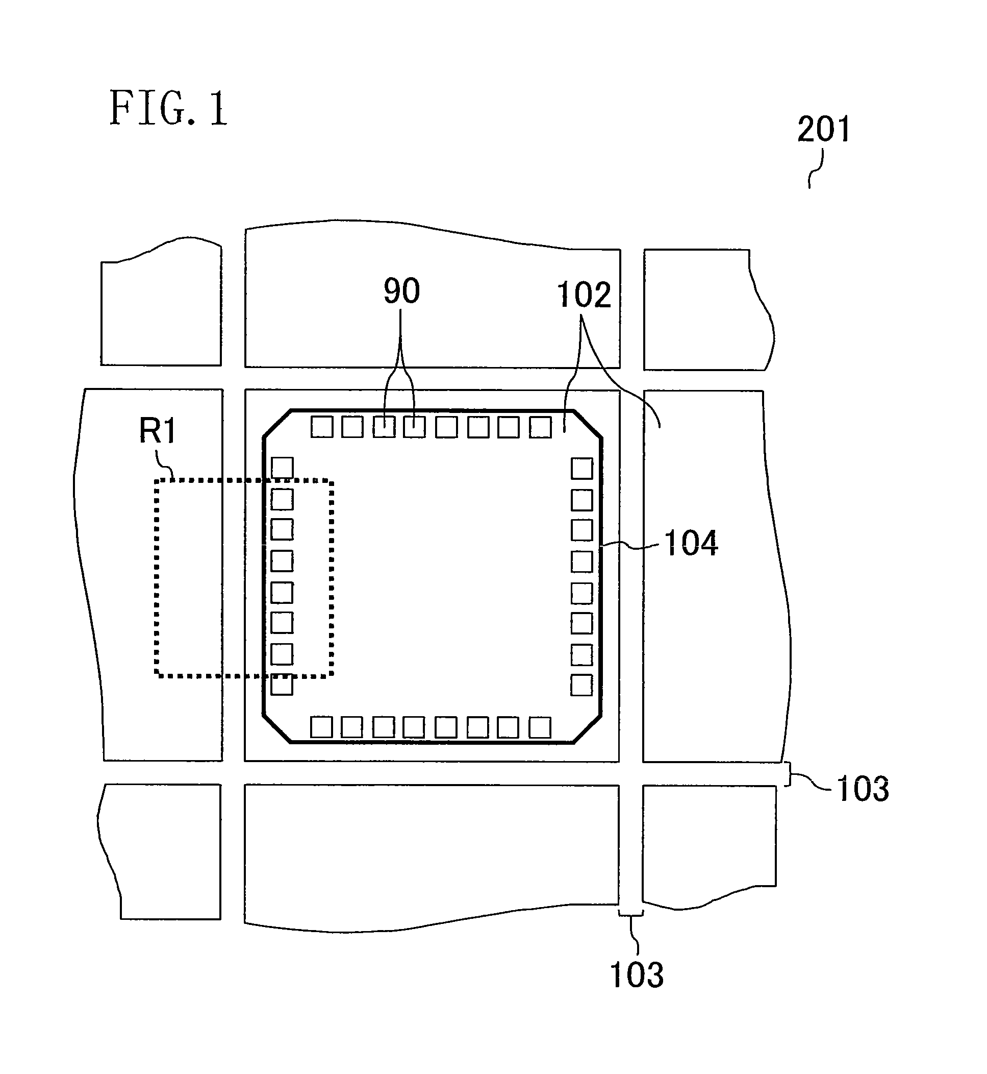
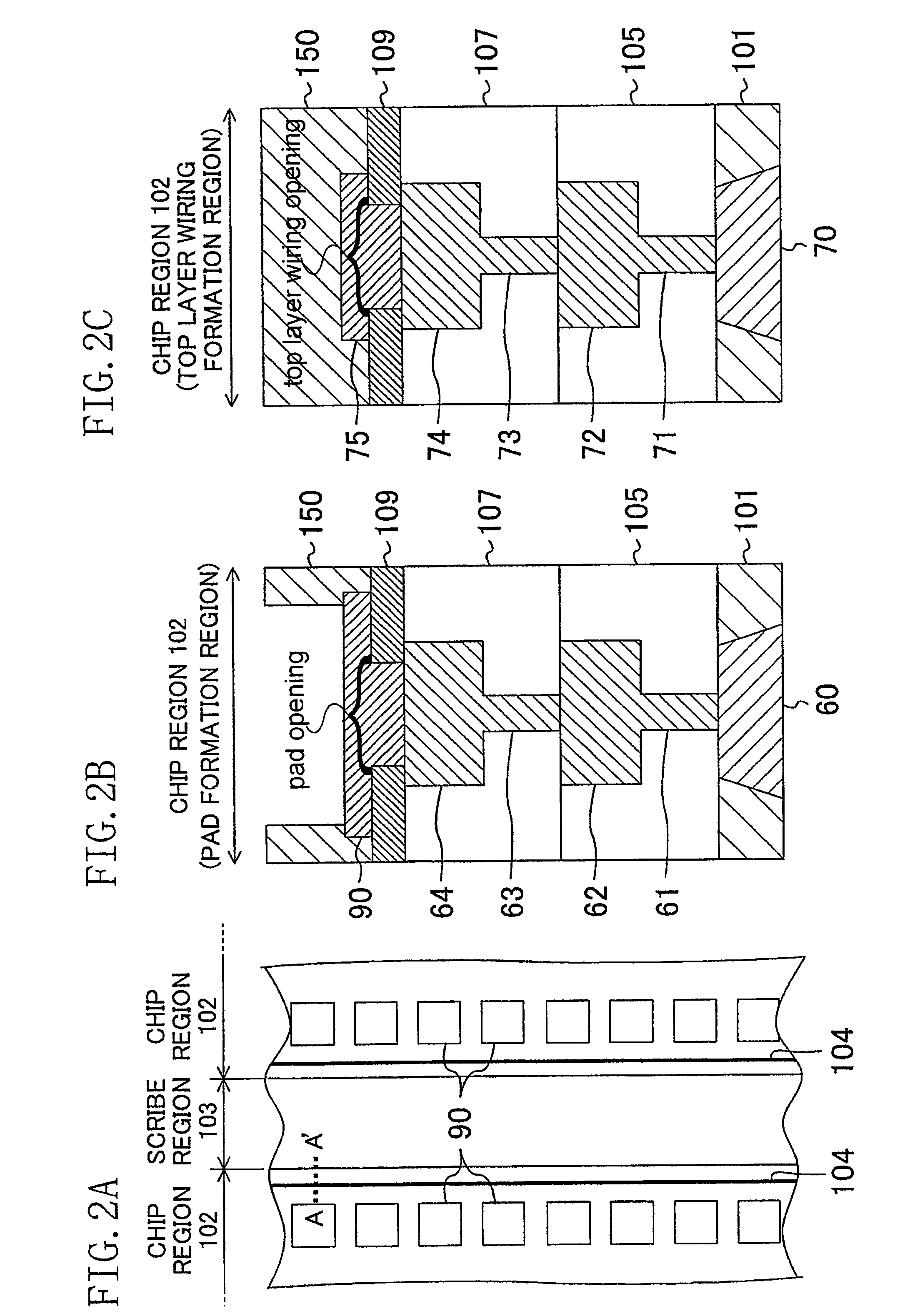
[0080]FIG. 3 shows a cross-sectional structure of an end portion of a semiconductor device (more specifically, a diced chip) according to the first embodiment. More specifically, FIG. 3 shows a cross-sectional structure of an end portion of a semiconductor device including a seal ring 104 formed in the periphery of the chip region 102. FIG. 3 is a cross-sectional view taken along line A-A′ in FIG. 2A.

[0081]As shown in FIG. 3, a chip region 102 is formed adjacent to a scribe region 103 on a substrate 101. A first interlayer insulating film 105 and a second interlayer insulating film 107 are sequentially formed on the substrate 101. A seal ring 104 is formed in the layered structure of the interlayer insulating films 105 and 107. The seal ring 104 extends through this layered structure and ...

second embodiment

[0152](Second Embodiment)

[0153]Hereinafter, a semiconductor device and a manufacturing method thereof according to a second embodiment of the invention will be described with reference to the figures.

[0154]FIG. 11 shows a cross-sectional structure of an end portion of a semiconductor device (more specifically, a diced chip) according to the second embodiment. More specifically, FIG. 11 shows a cross-sectional structure of an end portion of a semiconductor device including a seal ring 104 formed in the periphery of the chip region 102 as shown in FIG. 1. FIG. 11 is a cross-sectional view taken along line A-A′ in FIG. 2A. In FIG. 11, the same elements as those of the semiconductor device of the first embodiment shown in FIG. 3 are denoted with the same reference numerals and description thereof will be omitted as appropriate.

[0155]This embodiment is different from the first embodiment in the following points: as shown in FIG. 11, the first passivation film 109 has an opening 132 in ad...

third embodiment

[0193](Third Embodiment)

[0194]Hereinafter, a semiconductor device and a manufacturing method thereof according to a third embodiment of the invention will be described with reference to the figures.

[0195]FIG. 18 shows a cross-sectional structure of an end portion of a semiconductor device (more specifically, a diced chip) according to the third embodiment. More specifically, FIG. 18 shows a cross-sectional structure of an end portion of a semiconductor device including a seal ring 104 formed in the periphery of the chip region 102 as shown in FIG. 1. FIG. 18 is a cross-sectional view taken along line A-A′ in FIG. 2A. In FIG. 18, the same elements as those of the semiconductor device of the first embodiment shown in FIG. 3 are denoted with the same reference numerals and description thereof will be omitted as appropriate.

[0196]This embodiment is different from the first embodiment in the following points: as shown in FIG. 18, the first passivation film 109 has an opening 132 in addit...


PUM


Abstract

A semiconductor device includes: an interlayer insulating film formed on a substrate; a wiring formed in the interlayer insulating film in a chip region of the substrate; a seal ring formed in the interlayer insulating film in a periphery of the chip region and continuously surrounding the chip region; and a first protective film formed on the interlayer insulating film having the wiring and the seal ring formed therein. A first opening is formed in the first protective film in a region located outside the seal ring when viewed from the chip region, and the interlayer insulating film is exposed in the first opening.

Description

BACKGROUND OF THE INVENTION[0001]1. Field of the Invention[0002]The invention relates to a semiconductor device having a seal ring surrounding a chip region and a manufacturing method thereof.[0003]2. Background Art[0004]A semiconductor device is commonly manufactured by arranging a multiplicity of ICs (integrated circuits), each formed by a plurality of elements and having a prescribed function, in a matrix pattern on a semiconductor wafer such as silicon.[0005]A multiplicity of chip regions on a wafer are separated from each other by a grid-like scribe region (a grid-like scribe line). After a multiplicity of chip regions are formed on a wafer by a semiconductor manufacturing process, the wafer is diced into individual chips along the scribe region, whereby semiconductor devices are formed.[0006]When the wafer is diced into individual chips, chip regions near the scribe line may be subjected to mechanical impact, and the diced cross sections of the separated chips, that is, the se...

Claims


Application Information

Patent Timeline
Patent Type & Authority Patents(United States)
IPC IPC(8): H01L23/544
CPCH01L23/562H01L23/585H01L2924/0002H01L2924/00
Inventor TAKEMURA, KOJIHIRANO, HIROSHIGEITOH, YUTAKASANO, HIKARIKOIKE, KOJI
Owner PANASONIC CORP
Learn More