Electric device comprising phase change material and heating element

a phase change material and heating element technology, applied in semiconductor devices, digital storage, instruments, etc., can solve the problems of further limit delamination and segregation of pcm electrodes, lower electrode temperature, etc., and achieve high electrical isolation, high thermal, and high electrical conductivity.

Inactive Publication Date: 2012-05-08
NXP BV
View PDF12 Cites 14 Cited by
  • Summary
  • Abstract
  • Description
  • Claims
  • Application Information

AI Technical Summary

Benefits of technology

[0017]Hereto the electric device according to the present invention is characterised in that, the resistor is arranged as a first line and the heating element is arranged as a second line, the first line being adapted to conduct the first current and the second line being adapted to conduct the second current, wherein the first line and the second line cross at a cross position of the switching zone. In effect, the high programming current does not run through the interface between the phase change material and the electrode interface, whereby delamination and segregation is much reduced. Moreover, in the electric device the heated volume is well defined by the crossing area of the heater and the phase change resistor. This allows the heated volume to be smaller, with the advantageous effect that the power needed for the phase change transition is lowered and the size of the heated volume around the phase change material can be reduced. Also the heat will sink more towards the perpendicular heater instead of via the phase change lines, resulting in a lower electrode temperature, which further limits delamination and segregation of the PCM electrodes improving a read-out procedure.
[0019]In another embodiment, the heater as well as the phase change resistor is preferably a “dog bone” shaped line structure, with their crossing position in the narrow regions of both “dog bone” parts. The broad ends provide good thermal and low-resistive electrical contact to their electrodes.
[0021]The heater may be in direct contact with the phase change resistor, or be separated from it with an intermediate layer, such as a dielectric insulator layer, to reduce, and preferably, prevent mixing of the phase change material with the electric heater material.
[0024]In another embodiment of the invention, the heating element is composed of at least two layers. The first layer of the at least two layers is positioned between the second layer of the at least two layers and the phase change material. This first layer transfers the heat generated in the second layer to the phase change layer. The first layer is an insulator with a sufficiently high electrical isolation, and is preferably composed of undoped silicon. The second layer has a sufficiently high thermal and a sufficiently high electrical conductivity, and is preferably composed of a silicide compound, or even more preferably of salicided undoped silicon. This isolates the second layer electrically from the phase change layer, while keeping good thermal contact. As a result, the high-power programming path through the second layer of the heater is well isolated from the phase change layer, and it can be optimized separately from the reading part. Moreover, parasitical leakage via the heater to the PCM material is much less, such that no area-consuming design solutions are needed. Additionally, the much better heat transfer (approximately a factor ten to hundred) of silicon compared to a SiO2 dielectric results in a much lower power consumption. As a beneficial side-effect, the structure also allows to form an extremely thin heater layer, as the salicidation process is well controlled. A thin heater has the benefit of enhanced current density and therefore increased Joule heating at a given current.

Problems solved by technology

Also the heat will sink more towards the perpendicular heater instead of via the phase change lines, resulting in a lower electrode temperature, which further limits delamination and segregation of the PCM electrodes improving a read-out procedure.

Method used


Image

  • Electric device comprising phase change material and heating element
  • Electric device comprising phase change material and heating element
  • Electric device comprising phase change material and heating element

Examples


Embodiment Construction

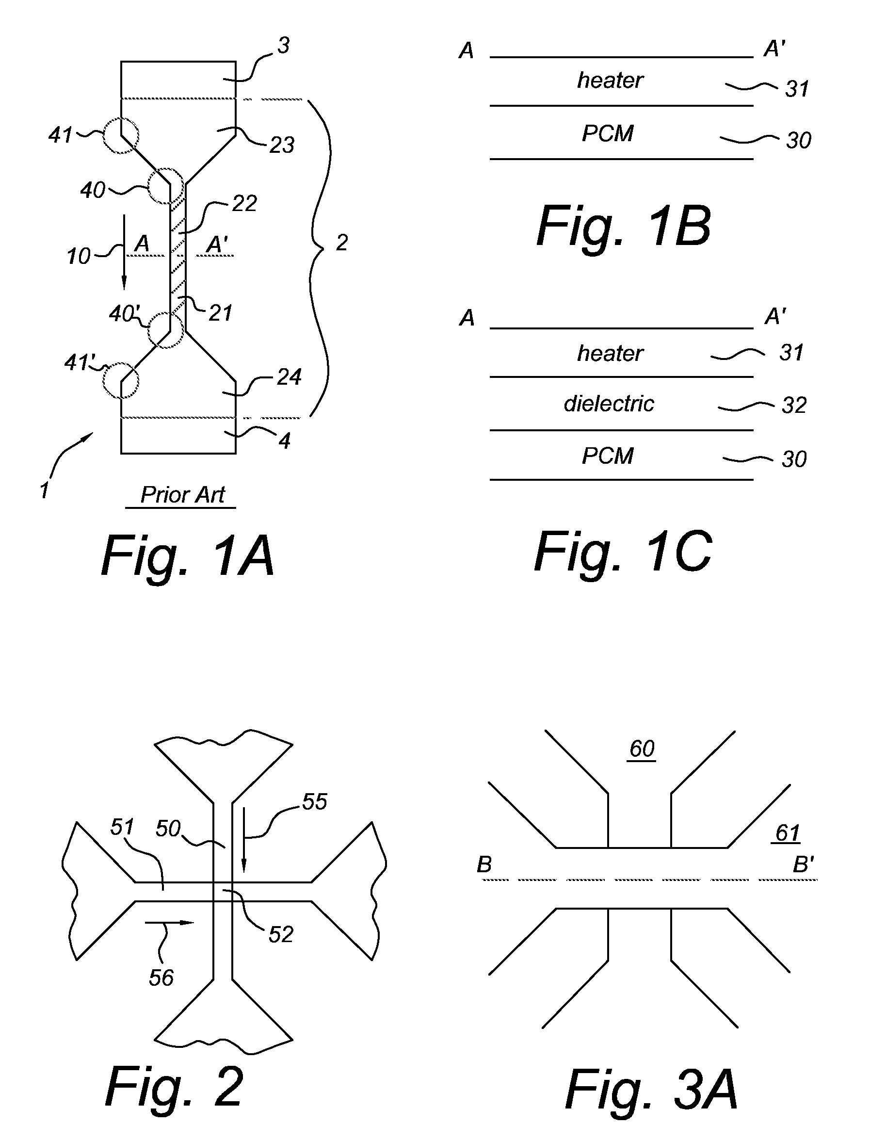
[0045]FIG. 1A shows a prior art resistor 1 which comprises a phase change material section 2, which is connected to the rest of the electric device via an electrode 3 and a counter electrode 4. A current path denoted by arrow 10 runs from the electrode 3 through the phase change material section 2 through electrode 4. The phase change material section 2 is deposited as a line on a substrate, such as a single crystal p-doped silicon semiconductor wafer. The phase change material is changeable between a first phase and a second phase. The resistor 1 has a first electrical resistance when the phase change material is in the first phase and a second electrical resistance, different from the first electrical resistance, when the phase change material is in the second phase. The phase change material section comprises a narrow part 21, which comprises a switching zone 22, and wide parts 23, 24. The wide parts 23, 24 connect the phase change material to the electrode 3 and the counter elec...


PUM


Abstract

An electric device has a resistor including a phase change material changeable between a first phase and a second phase within a switching zone. The resistor has a first resistance when the phase change material is in the first phase and a different second resistance, when the phase change material is in the second phase. The resistor may conduct a first current. The device has a heating element that may conduct a second current for enabling a transition of the phase change material from the first to the second phase. At the position of the switching zone, the resistor is arranged as a first line and the heating element is arranged as a second line. The first and second line may conduct the first current and the second current respectively, wherein the first line and the second line cross at the position of the switching zone.

Description

FIELD OF THE INVENTION[0001]The invention relates to an electric device comprising a resistor comprising a phase change material being changeable between a first phase and a second phase within a switching zone, the resistor having a first electrical resistance when the phase change material is in the first phase and a second electrical resistance, different from the first electrical resistance, when the phase change material is in the second phase, the resistor being capable of conducting a first current and the device having a heating element being able to conduct a second current for enabling a transition of the phase change material from the first phase to the second phase within the switching zone of the resistor.[0002]The invention also relates to a memory device comprising such an electric device, as well as an addressing method for programming such a memory device and an addressing method for reading such a memory device.[0003]The invention also relates to a semiconductor de...

Claims


Application Information

Patent Timeline
Patent Type & Authority Patents(United States)
IPC IPC(8): G11C11/00G11C7/00H01L21/02
CPCG11C13/0004G11C13/0069H01L27/2436H01L45/06H01L45/1206H01L45/1226H01L45/1286G11C2013/008G11C2213/79H10B63/30H10N70/253H10N70/823H10N70/8613H10N70/231
Inventor BAKS, WILKO
Owner NXP BV
Why Eureka
Try Eureka