Display device

a display device and display screen technology, applied in the field of display devices, can solve the problems of deterioration of outside light contrast, inability pixel defects, so as to enhance the view angle characteristics of white, reduce the pixel defects of organic el elements, and improve the effect of viewing angle characteristics

Inactive Publication Date: 2012-07-24
SONY CORP
View PDF4 Cites 10 Cited by
  • Summary
  • Abstract
  • Description
  • Claims
  • Application Information

AI Technical Summary

Benefits of technology

[0012]In the light of the foregoing, it is therefore desirable to provide a display device which is capable of reducing pixel defects of organic EL elements, and enhancing view angle characteristics of white which is easily visualized in terms of a visual feature of a human being without increasing a cost in a structure in which the organic EL elements, for emitting lights having the respective colors, each having a resonator structure are disposed.
[0014]In the display device having the structure described above, the cavity order of at least the light emitting element adapted to resonate the light, having the shortest wavelength (that is, the light emitting element having the shortest optical distance L in the cavity portion (the light emission functioning layer) when the cavity orders are identical to one another) of the light emitting elements corresponding to the respective colors and each having the cavity structure is 1, and the cavity order of each of other light emitting elements is 0. For this reason, the light emission functioning layer in at least the light emitting element having the cavity portion having the thinnest film thickness can be thickened to suppress the generation of the vanishing point while the deterioration of the view angle characteristics of the lights extracted from the light emitting elements, respectively, is suppressed. In addition thereto, the layers having the same structure and constituting the light emission functioning layer except for the light emitting layer in the light emitting elements are made the common layer. As a result, it is possible to approximate tendencies to show the dispersion in the total film thicknesses of the light emission functioning layers. Therefore, it is possible to enhance the view angle characteristics of white obtained by synthesizing the emitted lights corresponding to the respective colors.
[0015]As set forth hereinabove, according to the display device of an embodiment of the present invention, it is possible to reduce the pixel defects of the organic EL elements, and to enhance the view angle characteristics of white which is easily visualized in terms of the visual feature of a human being without increasing the cost in the color display device in which the organic EL elements corresponding to the respective colors and each having the resonator structure are disposed.

Problems solved by technology

The thinning of the organic layer causes a problem that pixel defects, such as a vanishing point, because an inter-electrode short-circuit generates.
In addition, with the structure described in Patent Document 3, it is necessary to newly form the concave structure, the light diffusing layer and the light deflecting layer, which leads to cost-up.
In addition, there is a new problem that an outside light is also scattered by the concave structure, the light diffusing layer and the light deflecting layer formed on the transparent substrate, so that an outside light contrast deteriorates remarkably.
In other words, even when the view angle characteristics of the organic EL element are improved every color, it may be impossible to enhance the view angle characteristics of white as long as there is the dispersion in the view angle characteristics of the colors.

Method used


Image

  • Display device
  • Display device
  • Display device

Examples


example 1

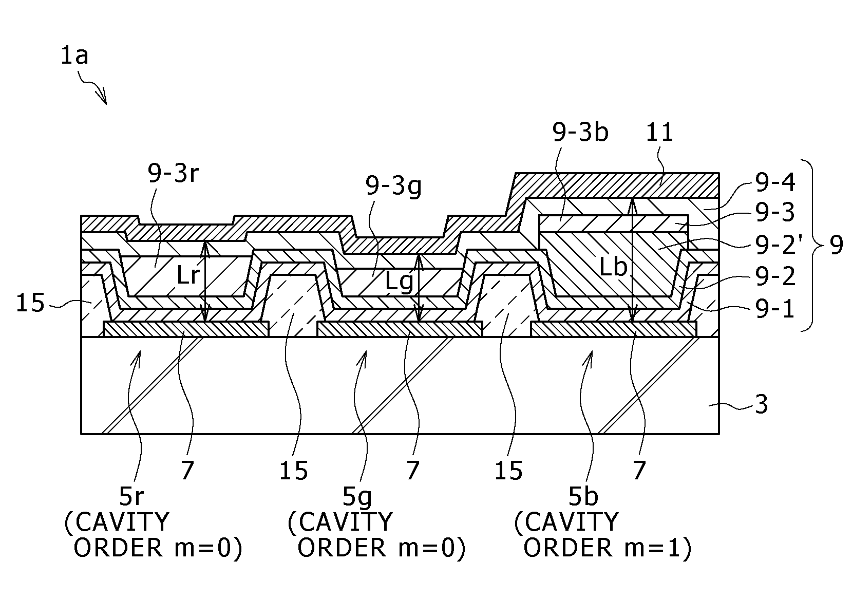
[0089]The display device 1a of the first embodiment previously described with reference to FIG. 1 was manufactured. As shown in TABLE 1, the film thicknesses of the layers constituting the light emission functioning layer 9 are set so that the cavity orders m of the light emitting elements 5r, 5g and 5b become 0, 0 and 1, respectively, by using the materials exemplified in the first embodiment.

[0090]

TABLE 1Example 1Film thickness (nm)FilmHoleHolethicknessLightElectronTotalinjectingtransportingadjustingemittingtransportingfilmCavitylayerlayerlayerlayerlayerthicknessorder m9-19-29-2′9-39-4(nm)Red02025—5025120(R)Green0—30100(G)Blue110026196(B)

[0091]The hole injecting layer 9-1, the hole transporting layer 9-2, the film thickness adjusting layer 9-2′, the light emitting layer 9-3, and the electron transporting layer 9-4 shown in TABLE 1 are deposited by utilizing a vacuum evaporation method. The film thickness adjusting layer 9-2′ of the blue light emitting element 5b, and the light emi...

example 2

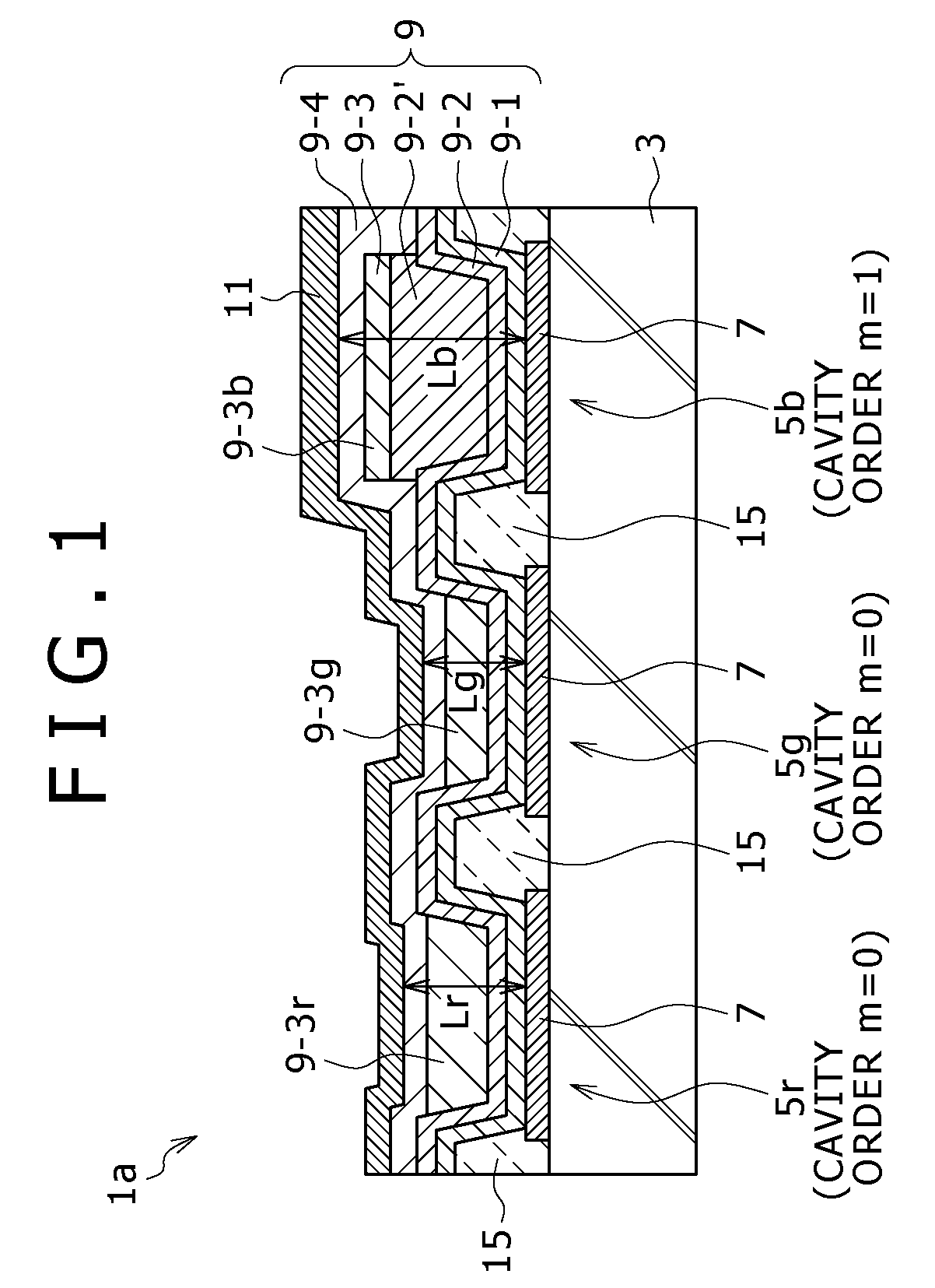
[0095]The display device 1b of the second embodiment previously described with reference to FIG. 2 is manufactured. As shown in TABLE 3, the film thicknesses of the layers constituting the light emission functioning layer 9 are set so that the cavity orders m of the light emitting elements 5r, 5g and 5b become 0, 1 and 1, respectively, by using the materials exemplified in the second embodiment.

[0096]

TABLE 3Example 2Film thickness (nm)FilmHoleHolethicknessLightElectronTotalinjectingtransportingadjustingemittingtransportingfilmCavitylayerlayerlayerlayerlayerthicknessorder m9-19-29-2′9-39-4(nm)Red02025—5025120(R)Green110080250(G)Blue126196(B)

[0097]The layers shown in TABLE 3 are deposited by utilizing the vacuum evaporation method. Also, the film thickness adjusting layers 9-2′ of the green light emitting element 5g and the blue light emitting element 5b are deposited in a pattern as the common layer by using the evaporation mask. Moreover, the light emitting layers 9-3r, 9-3g and 9-3...

example 3

[0101]The display device 1c of the third embodiment previously described with reference to FIG. 3 is manufactured. As shown in TABLE 3, the film thicknesses of the layers constituting the light emission functioning layer 9 are set so that the cavity orders m of the light emitting elements 5r, 5g and 5b become 1, 1 and 1, respectively by using the materials exemplified in the third embodiment.

[0102]

TABLE 5Example 3Film thickness (nm)FilmHoleHolethicknessLightElectronTotalinjectingtransportingadjustingemittingtransportingfilmCavitylayerlayerlayerlayerlayerthicknessorder m9-19-29-2′9-39-4(nm)Red120125508025300(R)Green130250(G)Blue1—26196(B)

[0103]The layers shown in TABLE 5 are deposited by utilizing the vacuum evaporation method. Also, the film thickness adjusting layers 9-2′ of the red light emitting element 5r and the green light emitting element 5g are deposited in a pattern as the common layer by using the evaporation mask. Moreover, the light emitting layers 9-3r, 9-3g and 9-3b ar...


PUM


Abstract

A display device includes light emitting elements corresponding to respective colors disposed on a substrate. Each of the light emitting elements corresponding to the respective colors has a cavity structure in which a light emission functioning layer including a light emitting layer is held between a reflecting electrode and a semitransmitting electrode. A cavity order of at least the light emitting element adapted to resonate a light, having the shortest wavelength, of the light emitting elements corresponding to the respective colors is 1, and a cavity order of each of other light emitting elements is 0. The light emission functioning layer except for the light emitting layer is common to the light emitting elements corresponding to the respective colors.

Description

CROSS REFERENCES TO RELATED APPLICATIONS[0001]The present invention contains subject matter related to Japanese Patent Application JP 2007-293814 filed in the Japan Patent Office on Nov. 13, 2007, the entire contents of which being incorporated herein by reference.BACKGROUND OF THE INVENTION[0002]1. Field of the Invention[0003]The present invention relates to a display device in which self-light emission type elements such as organic electroluminescence (EL) elements are disposed, and more particularly to a display device in which elements, for emitting lights having respective colors, each having a cavity structure are provided.[0004]2. Description of Related Art[0005]In recent years, an organic electroluminescence (EL) display device using organic EL elements has been put into practical use as a display device substituted for a liquid crystal display device. The organic EL display device has a wider view angle than that in the liquid crystal display device because it is of a self-...

Claims


Application Information

Patent Timeline
Patent Type & Authority Patents(United States)
IPC IPC(8): H01L29/08H01L51/00H01L35/24H01L51/50H05B33/24
CPCH01L51/5265H01L27/3211H01L27/3244H10K59/35H10K59/12H10K50/852H10K50/13H10K50/15H10K50/16
Inventor ASAKI, REOYAMADA, JIRO
Owner SONY CORP
Why Eureka
Try Eureka