Liquid crystal display device

Inactive Publication Date: 2005-09-15
FUJITSU LTD +1
View PDF5 Cites 22 Cited by
  • Summary
  • Abstract
  • Description
  • Claims
  • Application Information

AI Technical Summary

Benefits of technology

[0032] However, light transmittance is reduced when the slit width S exceeds 4 μm, and liquid crystal molecules cannot be tilted in predetermined directions when the slit width S exceeds 7 μm. Accordingly, the slit width S is preferably set to 7 μm or less, more preferably 4 μm or less. Moreover, light transmittance is sharply reduced when the distance L between the slits exceeds 6 μm, and disclination occurs on the electrode when th

Problems solved by technology

However, TN-mode liquid crystal display devices have the disadvantage that viewing angle characteristics are poor and that contrast and color greatly change when a screen is viewed from an oblique direction.
However, since the aperture ratio is significantly reduced by the comb-shaped electrode, there is a drawback in that a strong backlight is required.
However, also in the case of an MVA-mode liquid crystal display device, since the aperture ratio is reduced by protrusions and slits though less than that of an IPS-mode liquid crystal display device, the light transmittance is low compared to that of a TN-mode liquid crystal display device.
Accordingly, it i

Method used


Image

  • Liquid crystal display device
  • Liquid crystal display device
  • Liquid crystal display device

Examples


first embodiment

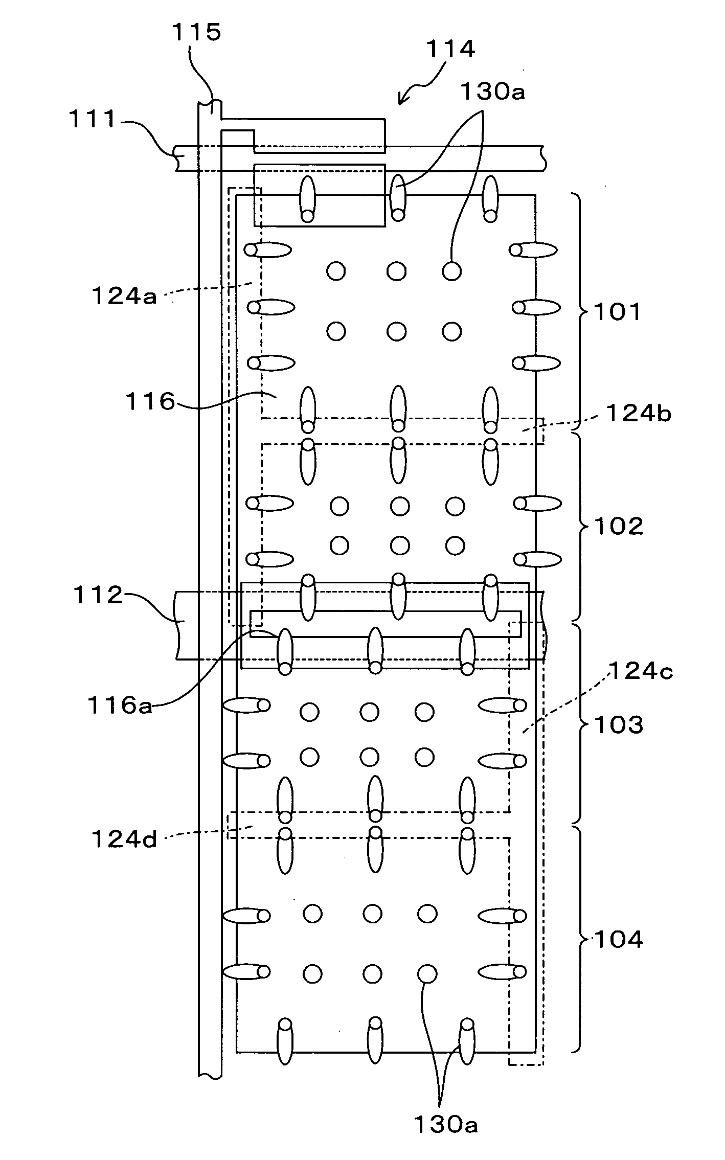
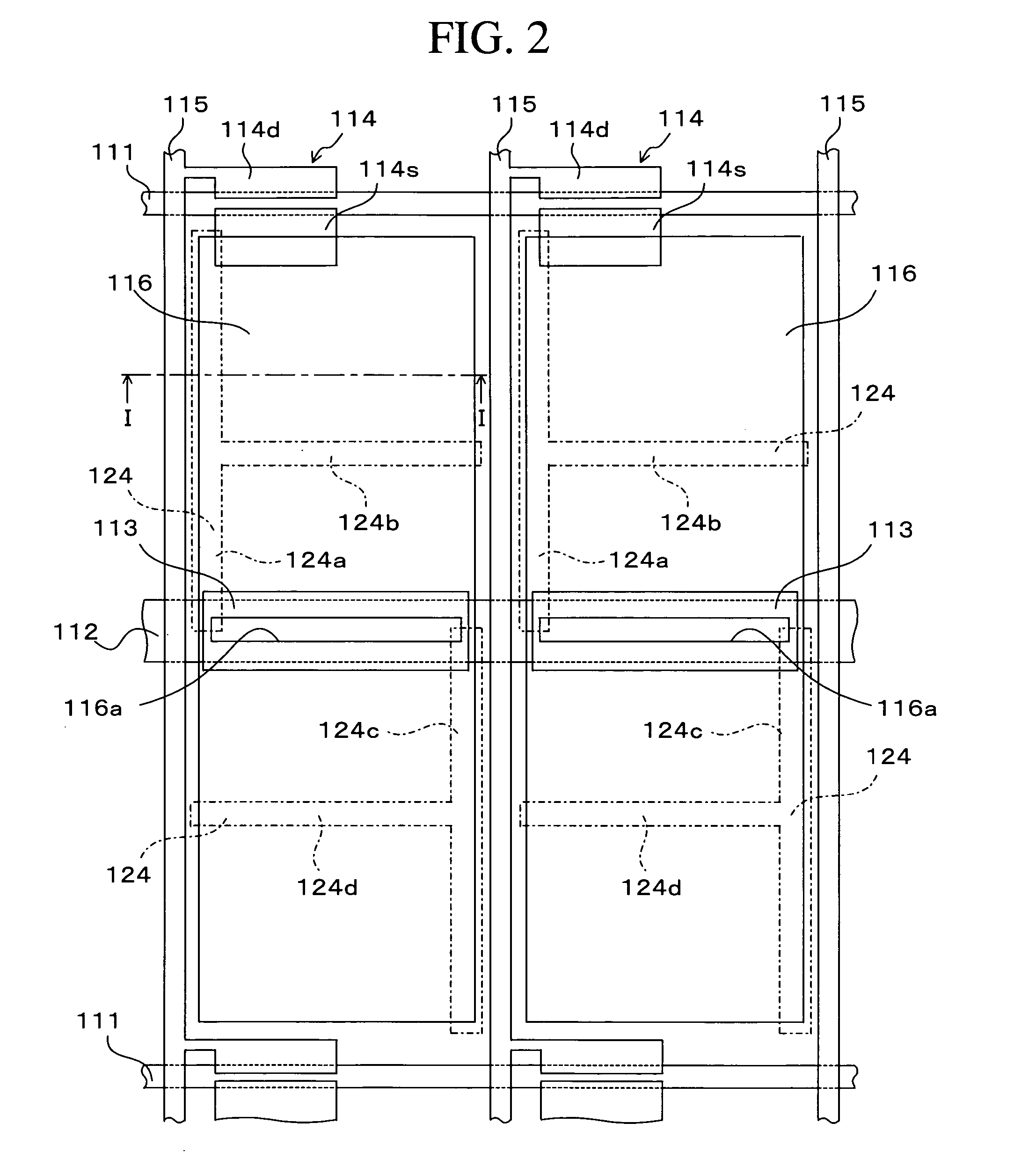
[0060]FIG. 2 is a plan view showing a liquid crystal display device of a first embodiment of the present invention. In this FIG. 2, two picture elements provided on a TFT substrate are shown. Further, in FIG. 3, a schematic cross section taken along the I-I line of FIG. 2 is shown. Note that numeric values in the following description are examples in the case of an XGA (1024×768 pixels) liquid crystal display device in which the panel size is 15 inches and in which the cell gap is 3.8 to 4.4 μm.

[0061] On the TFT substrate 110, a plurality of horizontally extending gate bus lines 111 and a plurality of vertically extending data bus lines 115 are formed. Each of the rectangular areas defined by the gate and data bus lines 111 and 115 is a picture element area. Further, on the TFT substrate 110, auxiliary capacitance bus lines 112, which are placed parallel to the gate bus lines 111 and cross the centers of the picture element areas, are formed. A first insulating film (not shown) is ...

second embodiment

[0096] Hereinafter, a second embodiment will be described.

[0097] In the first embodiment, it is considered that, as shown in FIG. 8, for example, in the first area 101, the liquid crystal molecules 130a in the middle portions of the protrusions 124a, 124b, and the like and the middle portions of the edges of the picture element electrodes 116 (regions surrounded by broken lines in the drawing) are tilted in directions shifted from 45°, because the force which tends to tilt the liquid crystal molecules 130a downward and the force which tends to tilt the liquid crystal molecules 130a leftward are not equivalent. In the case where the liquid crystal molecules 130a are aligned as in this FIG. 8, a region with low transmittance occurs in the middle portion of each side of the first area 101 as shown in FIG. 9. This tendency becomes more prominent as the lengths of the sides of the first area 101 become longer.

[0098] Accordingly, in the second embodiment, as shown in FIG. 10, slits (obl...

third embodiment

[0103]FIG. 11 is a plan view showing a liquid crystal display device of a third embodiment of the present invention. Incidentally, the third embodiment differs from the second embodiment in that the pattern of slits formed in picture element electrodes and the pattern of protrusions formed on a counter substrate differ from those of the second embodiment. Except for this, the configuration is basically the same as that of the second embodiment. Accordingly, in FIG. 11, the same components as those in FIG. 10 are denoted by the same reference numerals, and will not be further described in detail. Further, in FIG. 11, auxiliary capacitance bus lines and auxiliary capacitance electrodes are not shown.

[0104] In the present embodiment, a protrusion 124e is formed along the upper half of the left edge of each picture element electrode 116, and a protrusion 124f is formed along the lower half of the right edge of each picture element electrode 116. Further, a protrusion 124g is formed alo...


PUM

PropertyMeasurementUnit
Lengthaaaaaaaaaa
Lengthaaaaaaaaaa
Lengthaaaaaaaaaa

Abstract

In the middle of each picture element electrode on a TFT substrate, a slit parallel to gate bus lines is formed. On a counter substrate, protrusions are formed. Each protrusion includes a protrusion placed along the left edge of the upper half of a picture element electrode, a protrusion horizontally extending from the middle of the preceding protrusion, a protrusion placed along the right edge of the lower half of the picture element electrode, and a protrusion horizontally extending from the middle of the preceding protrusion. Liquid crystal molecules are aligned with directions of approximately 45° relative to the protrusions and the edges of the picture element electrodes.

Description

CROSS-REFERENCE TO RELATED APLICATIONS [0001] This application is based on and claims priority of Japanese Patent Application No. 2004-071178 filed on Mar. 12, 2004, the entire contents of which are incorporated herein by reference. BACKGROUND OF THE INVENTION [0002] 1. Field of the Invention [0003] The present invention relates to a multi-domain vertical alignment (MVA) mode liquid crystal display device having, within each picture element, multiple domains where the alignment directions of liquid crystal molecules are different from each other. [0004] 2. Description of the Prior Art [0005] Liquid crystal display devices have the advantages in that they are thin and light in weight compared to cathode-ray tube (CRT) displays and that they can be driven at low voltages to have low power consumption. Accordingly, liquid crystal display devices are used in various kinds of electronic devices including televisions, notebook personal computers (PCs), desktop PCs, personal digital assist...

Claims


Application Information

Patent Timeline
IPC IPC(8): G02F1/1337G02F1/1343
CPCG02F1/133707G02F2201/40G02F2001/13775G02F2001/13712G02F1/13712G02F1/13775
Inventor NAKANISHI, YOHEI
Owner FUJITSU LTD
Why Eureka
Try Eureka