Display device

a display device and display technology, applied in the field of display devices, can solve the problems of deterioration of outside light contrast, pixel defects, and inability so as to enhance the view angle characteristics of white, reduce the pixel defects of organic el elements, and improve the effect of viewing angle characteristics

Inactive Publication Date: 2009-05-14
SONY CORP
View PDF1 Cites 31 Cited by
  • Summary
  • Abstract
  • Description
  • Claims
  • Application Information

AI Technical Summary

Benefits of technology

[0014]In the display device having the structure described above, the cavity order of at least the light emitting element adapted to resonate the light, having the shortest wavelength (that is, the light emitting element having the shortest optical distance L in the cavity portion (the light emission functioning layer) when the cavity orders are identical to one another) of the light emitting elements corresponding to the respective colors and each having the cavity structure is 1, and the cavity order of each of other light emitting elements is 0. For this reason, the light emission functioning layer in at least the light emitting element having the cavity portion having the thinnest film thickness can be thickened to suppress the generation of the vanishing point while the deterioration of the view angle characteristics of the lights extracted from the light emitting elements, respectively, is suppressed. In addition thereto, the layers having th

Problems solved by technology

The thinning of the organic layer causes a problem that pixel defects, such as a vanishing point, because an inter-electrode short-circuit generates.
In addition, with the structure described in Patent Document 3, it is necessary to newly form the concave structure, the light diffusing layer and the light deflecting layer, which leads to cost-up.
In addition, there is a new problem that an outside light is also scattered by the co

Method used


Image

  • Display device
  • Display device
  • Display device

Examples


first embodiment

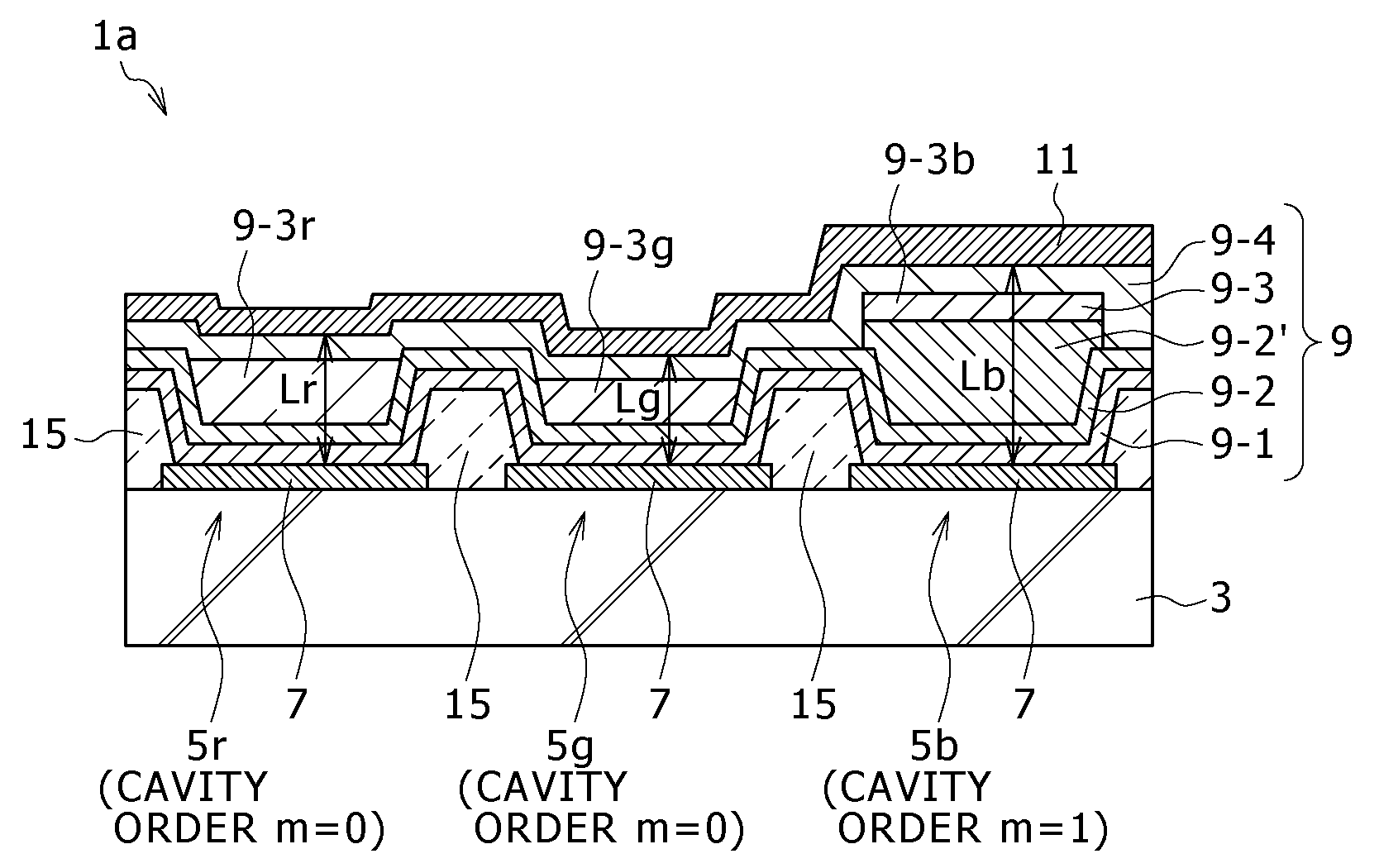
[0027]FIG. 1 is a cross sectional view of a main portion explaining a display device according to a first embodiment of the present invention. In a display device 1a shown in the figure, organic EL elements 5r, 5g and 5b for emitting lights having colors of red (R), green (G) and blue (B), respectively, that is, the red light emitting element 5r, the green light emitting element 5g and the blue light emitting element 5b are disposed in a matrix on a substrate 3. Also, the display device 1a is structured as an upper surface emission type display device in which the lights emitted from the light emitting elements 5r, 5g and 5b, respectively, are extracted from a side opposite to the substrate 3.

[0028]The substrate 3 is a so-called thin film transistor (TFT) substrate obtained by disposing and forming TFT transistors (not shown) on a surface layer of a glass substrate, a silicon substrate, a plastic substrate or the like. Also, a surface of the substrate 3 is covered with a planarizati...

second embodiment

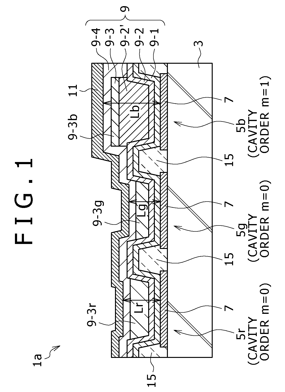
[0060]FIG. 2 is a cross sectional view of a main portion explaining a display device according to a second embodiment of the present invention. A display device 1b of the second embodiment shown in FIG. 2 is different from the display device 1a of the first embodiment in that the cavity orders m of the blue light emitting element 5b and the green light emitting element 5g are each set to 1, and the cavity order of the red light emitting element 5r is set to 0, and moreover the layer structure for realizing this is obtained. Other structures of the display device 1b of the second embodiment are the same as those of the display device 1a of the first embodiment.

[0061]Optical distances Lr, Lg and Lb in the light emitting elements 5r, 5g and 5b in which the cavity orders m are set to 0, 1 and 1, respectively, as described above are adjusted based on the film thicknesses of the light emitting layers 9-3r, 9-3g and 9-3b corresponding to the respective colors together with the film thickne...

third embodiment

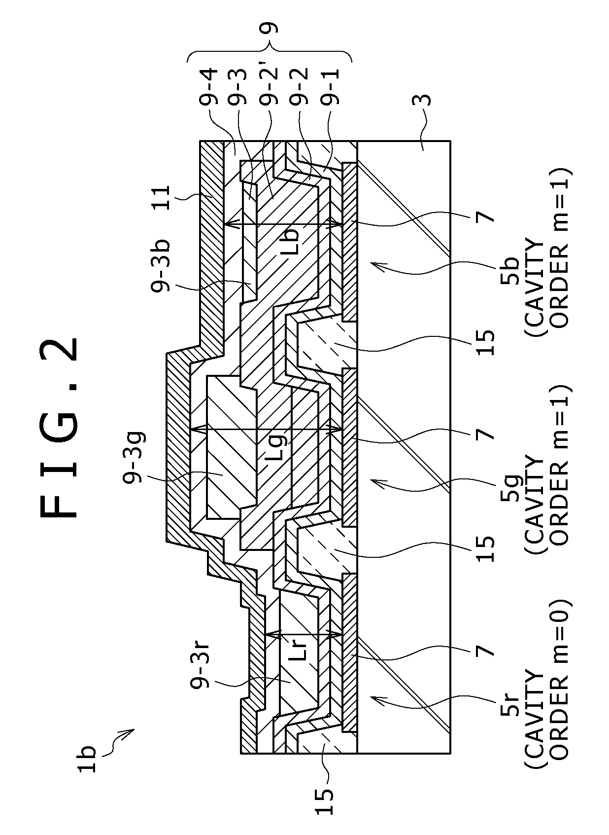
[0065]FIG. 3 is a cross sectional view of a main portion explaining a display device according to a third embodiment of the present invention. A display device 1c of the third embodiment shown in FIG. 3 is different from the display device 1a of the first embodiment in that the cavity orders m of the light emitting elements 5r, 5g and 5b, corresponding to the respective colors, including the blue light emitting element 5b are each set to 1, and moreover the layer structure for realizing this is obtained. Other structures of the display device 1c of the third embodiment are the same as those of the display device 1a of the first embodiment.

[0066]Optical distances Lr, Lg and Lb in the light emitting elements 5r, 5g and 5b in which the cavity orders m are set to 1, 1 and 1, respectively, as described above are adjusted based on film thicknesses of light emitting layers 9-3r, 9-3g and 9-3b corresponding to the respective colors. In addition, in the third embodiment, in order to realize ...


PUM


Abstract

A display device includes light emitting elements corresponding to respective colors disposed on a substrate. Each of the light emitting elements corresponding to the respective colors has a cavity structure in which a light emission functioning layer including a light emitting layer is held between a reflecting electrode and a semitransmitting electrode. A cavity order of at least the light emitting element adapted to resonate a light, having the shortest wavelength, of the light emitting elements corresponding to the respective colors is 1, and a cavity order of each of other light emitting elements is 0. The light emission functioning layer except for the light emitting layer is common to the light emitting elements corresponding to the respective colors.

Description

CROSS REFERENCES TO RELATED APPLICATIONS[0001]The present invention contains subject matter related to Japanese Patent Application JP 2007-293814 filed in the Japan Patent Office on Nov. 13, 2007, the entire contents of which being incorporated herein by reference.BACKGROUND OF THE INVENTION[0002]1. Field of the Invention[0003]The present invention relates to a display device in which self-light emission type elements such as organic electroluminescence (EL) elements are disposed, and more particularly to a display device in which elements, for emitting lights having respective colors, each having a cavity structure are provided.[0004]2. Description of Related Art[0005]In recent years, an organic electroluminescence (EL) display device using organic EL elements has been put into practical use as a display device substituted for a liquid crystal display device. The organic EL display device has a wider view angle than that in the liquid crystal display device because it is of a self-...

Claims


Application Information

Patent Timeline
IPC IPC(8): H01L27/15H01L51/50H05B33/24
CPCH01L27/3211H01L51/5265H01L27/3244H10K59/35H10K59/12H10K50/852H10K50/13H10K50/15H10K50/16
Inventor ASAKI, REOYAMADA, JIRO
Owner SONY CORP
Why Eureka
Try Eureka