Display device and display unit

a display device and display unit technology, applied in static indicating devices, instruments, optical elements, etc., can solve the problems of deteriorating the outside light contrast, lowering the image quality and the like, and deteriorating the view angle characteristics, so as to improve the front-facing light extraction efficiency and improve the view angle characteristics. , the effect of reducing the light emitting intensity

Active Publication Date: 2008-06-19
SONY CORP
View PDF10 Cites 56 Cited by
  • Summary
  • Abstract
  • Description
  • Claims
  • Application Information

AI Technical Summary

Benefits of technology

[0007]When the resonator structure is provided for the organic light emitting device, since a spectrum of resonated light has a high and narrow peak, the light extraction efficiency in the front direction to the display screen is improved. However, when the screen is viewed from an oblique direction, the light emitting wavelength is largely shifted and the light emitting intensity is lowered. That is, in the past, luminance difference and color shift are generated according to the viewing angle to the screen, leading to deterioration of the view angle characteristics, lowering of the image quality and the like.

Problems solved by technology

That is, in the past, luminance difference and color shift are generated according to the viewing angle to the screen, leading to deterioration of the view angle characteristics, lowering of the image quality and the like.
However, in such an existing method, there has been a disadvantage that outside light is also scattered by the concave structure, the light diffusion layer, and the light refraction layer formed on the transparent substrate, leading to largely deteriorating the outside light contrast.
It results in necessity of a film forming process and a patterning process thereof, leading to increase of the manufacturing cost.
Further, a step where the thickness of the transparent conductive film is changed is likely to become a cause of non-light emitting defect or the like.
However, it causes lowering of aperture ratio.

Method used


Image

  • Display device and display unit
  • Display device and display unit
  • Display device and display unit

Examples


first embodiment

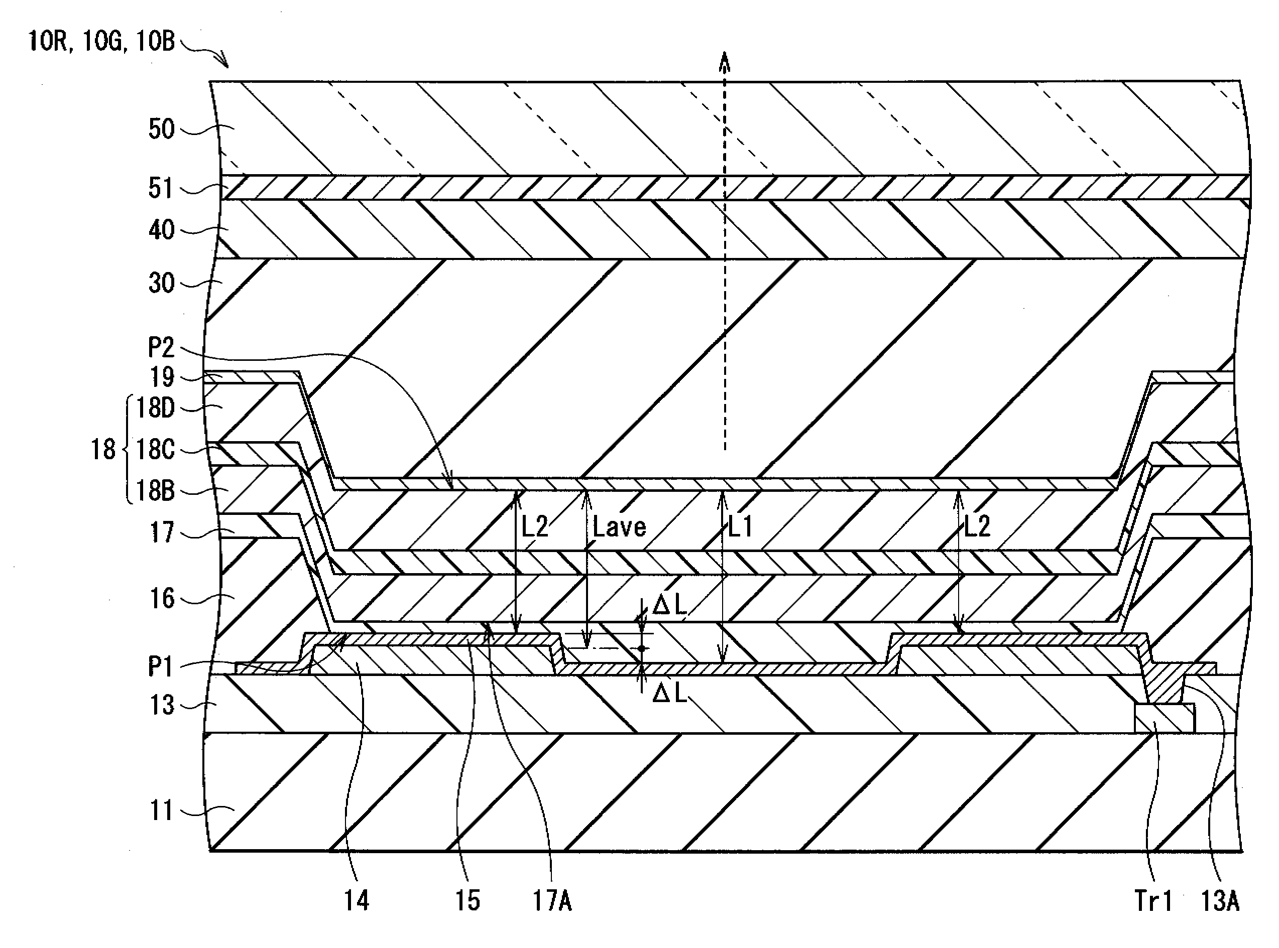
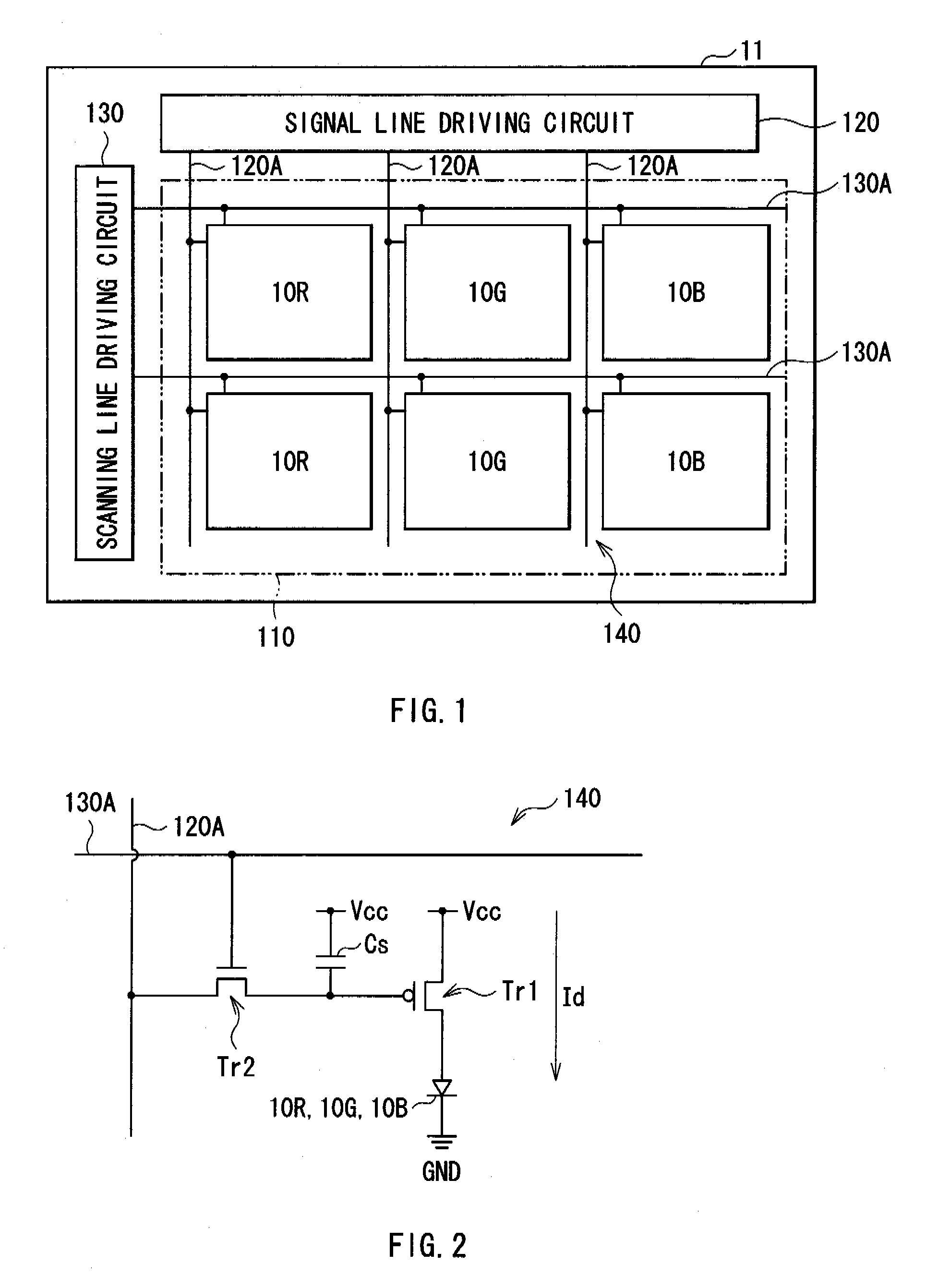
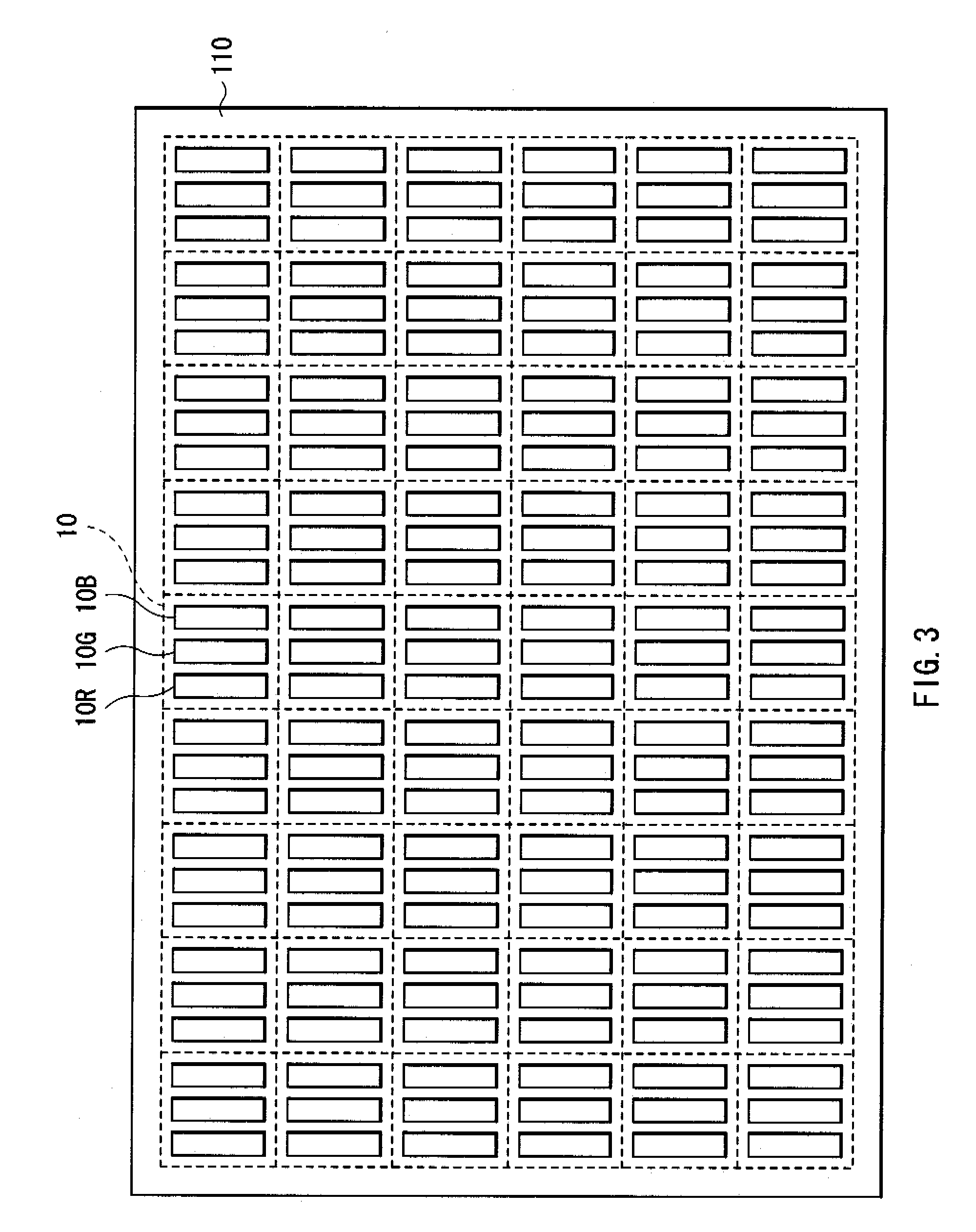
[0066]FIG. 1 shows a configuration of a display unit using an organic light emitting device according to a first embodiment of the invention. The display unit is used as an ultrathin organic light emitting color display unit or the like. For example, a display region 110 in which a plurality of organic light emitting devices 10R, 10G and 10B described later are arranged in a matrix state is formed on a substrate 11 made of glass, a silicon (Si) wafer, a resin or the like. A signal line driving circuit 120 and a scanning line driving circuit 130 that are drivers for displaying an image are formed on the periphery of the display region 110.

[0067]In the display region 110, a pixel driving circuit 140 is formed. FIG. 2 shows an example of the pixel driving circuit 140. The pixel driving circuit 140 is formed in a layer lower than a first electrode 15 described later. The pixel driving circuit 140 is an active driving circuit having a driving transistor Tr1, a writing transistor Tr2, a c...

second embodiment

[0113]FIG. 13 shows a cross sectional structure of the organic light emitting devices 10R, 10G and 10B of a display unit according to a second embodiment of the invention. The organic light emitting devices 10R, 10G and 10B of the display unit according to the second embodiment is the same as those of the display unit described in the first embodiment, except that an arrangement relation between the driving transistor Tr1 of the pixel driving circuit 140 and the first electrode 15 is adjusted so that a step is formed on the interface of the first electrode 15 on the light emitting layer 18C side, and the step forming layer 14 is not provided. Therefore, a description will be given by affixing the same symbols to the same elements as those of the first embodiment.

[0114]The driving transistor Tr1 is provided in the second region 22 on the substrate 11. By providing a sufficient large step formed by the driving transistor Tr1, a step reflecting the driving transistor Tr1 is left on the...

third embodiment

[0127]FIG. 14 shows a cross sectional structure of the organic light emitting devices 10R, 10G and 10B of a display unit according to a third embodiment of the invention. The organic light emitting devices 10R, 10G and 10B of the display unit according to the third embodiment are the same as those of the display unit described in the first embodiment, except that the step forming layer 14 is made of the same material as that of the driving transistor Tr1. Therefore, a description will be given by affixing the same symbols to the same elements as those of the first embodiment.

[0128]The step forming layer 14 is provided in the second region 22 on the substrate 11. The step forming layer 14 is made of the same material as that of the source wiring 156S and the drain wiring 156D of the driving transistor Tr1. That is, the step forming layer 14 has a structure in which a titanium (Ti) layer 166A, an aluminum (Al) layer 166B, a titanium (Ti) layer 166C, and the protective film 157 are lay...


PUM


Abstract

A display device capable of improving the view angle characteristics without deteriorating the outside light contrast and a display unit using it are provided. The display device includes a first electrode, an organic layer including a light emitting lay and a second electrode sequentially over a substrate, and having a resonator structure in which light generated in the light emitting layer is resonated between a first end and a second end. An end face of the first electrode on the light emitting layer side is the first end having a step shape. A distance adjustment layer that fills in the step shape and has a flat surface on the second electrode side is provided between the first electrode and the second electrode, and thereby the second end is planarized, and an optical distance between the first end and the second end is varied according to the step shape.

Description

CROSS REFERENCES TO RELATED APPLICATIONS[0001]The present invention contains subject matter related to Japanese Patent Application JP 2006-027062 filed in the Japanese Patent Office on Feb. 3, 2006, and Japanese Patent Application JP 2006-351863 filed in the Japanese Patent Office on Dec. 27, 2006, the entire contents of which being incorporated herein by references.BACKGROUND OF THE INVENTION[0002]1. Field of the Invention[0003]The present invention relates to a self-light emitting display device such as an organic light emitting device and a display unit, and particularly to a display device having a resonator structure and a display unit.[0004]2. Description of the Related Art[0005]In these years, as a display unit displacing a liquid crystal display, an organic EL display using organic light emitting devices has been in practical use. Since the organic EL display is a self-light emitting display, its view angle is wider than that of the liquid crystal display. Further, the organ...

Claims


Application Information

Patent Timeline
Patent Type & Authority Applications(United States)
IPC IPC(8): G02B5/00H01L51/50G09G3/30
CPCG09G3/3225G09G2320/028H01L51/5265H01L51/5203H01L27/3244H10K59/12H10K50/813H10K50/852H10K59/805H05B33/22H05B33/20H10K50/805
Inventor ASAKI, REOFUJIOKA, HIROFUMIHIROMASU, YASUNOBU
Owner SONY CORP
Why Eureka
Try Eureka