Light emitting element driving circuit

a technology of light emitting elements and driving circuits, applied in the direction of electric variable regulation, process and machine control, instruments, etc., can solve the problems of reducing the responsivity of the driving circuit, increasing the system cost, and ld degradation, so as to improve the control accuracy of the pulse width, reduce the effect of overshoot and undershoo

Inactive Publication Date: 2013-01-22
CANON KK
View PDF7 Cites 3 Cited by
  • Summary
  • Abstract
  • Description
  • Claims
  • Application Information

AI Technical Summary

Benefits of technology

[0007]According to one aspect of the present invention, in consideration of the problems in the prior art, there is provided a light emitting element driving circuit which improves the control accuracy of the pulse width of light emitted by an LD based on a data signal, allows low-voltage operation, and suppresses overshoot and undershoot in an output current.

Problems solved by technology

This leads to an increase in system cost.
This causes overshoot, undershoot, and ringing in the waveform of a constant current supplied to the LD, resulting in degradation of the LD.
This makes it necessary to drive “the MOS transistor designed with a necessary size” with a small current in a low-current region, as described above, resulting in a degradation in the responsivity of the driving circuit.
Since a parasitic capacitance including the gate capacitance of “MOS transistor designed with a necessary size” is charged, the rising time increases, resulting in a failure to obtain a desired optical pulse width.
When using a cathode common LD, it is necessary to use a PMOS which is inferior in current supplying ability or current driving ability to an NMOS.

Method used


Image

  • Light emitting element driving circuit
  • Light emitting element driving circuit
  • Light emitting element driving circuit

Examples


first embodiment

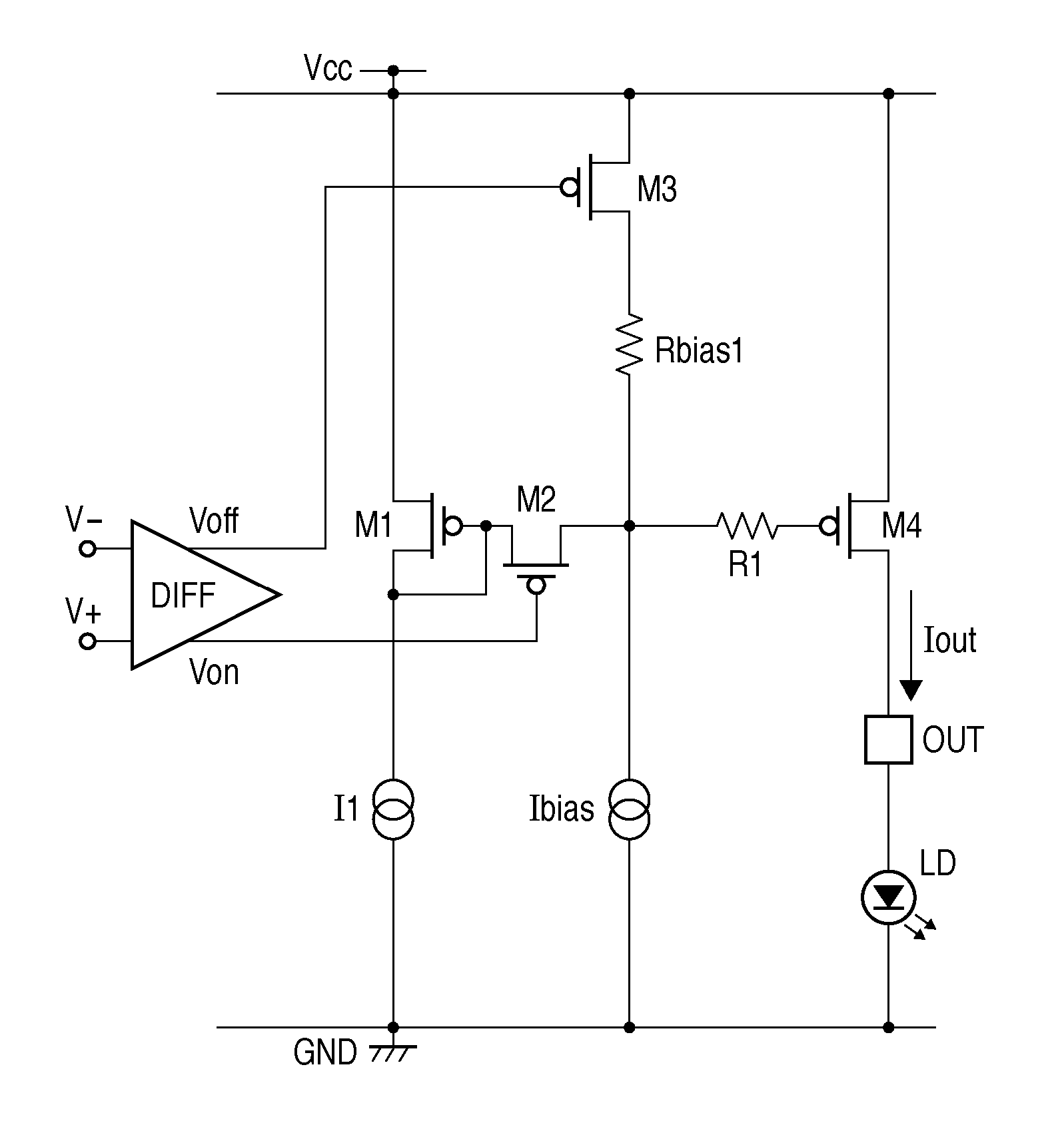
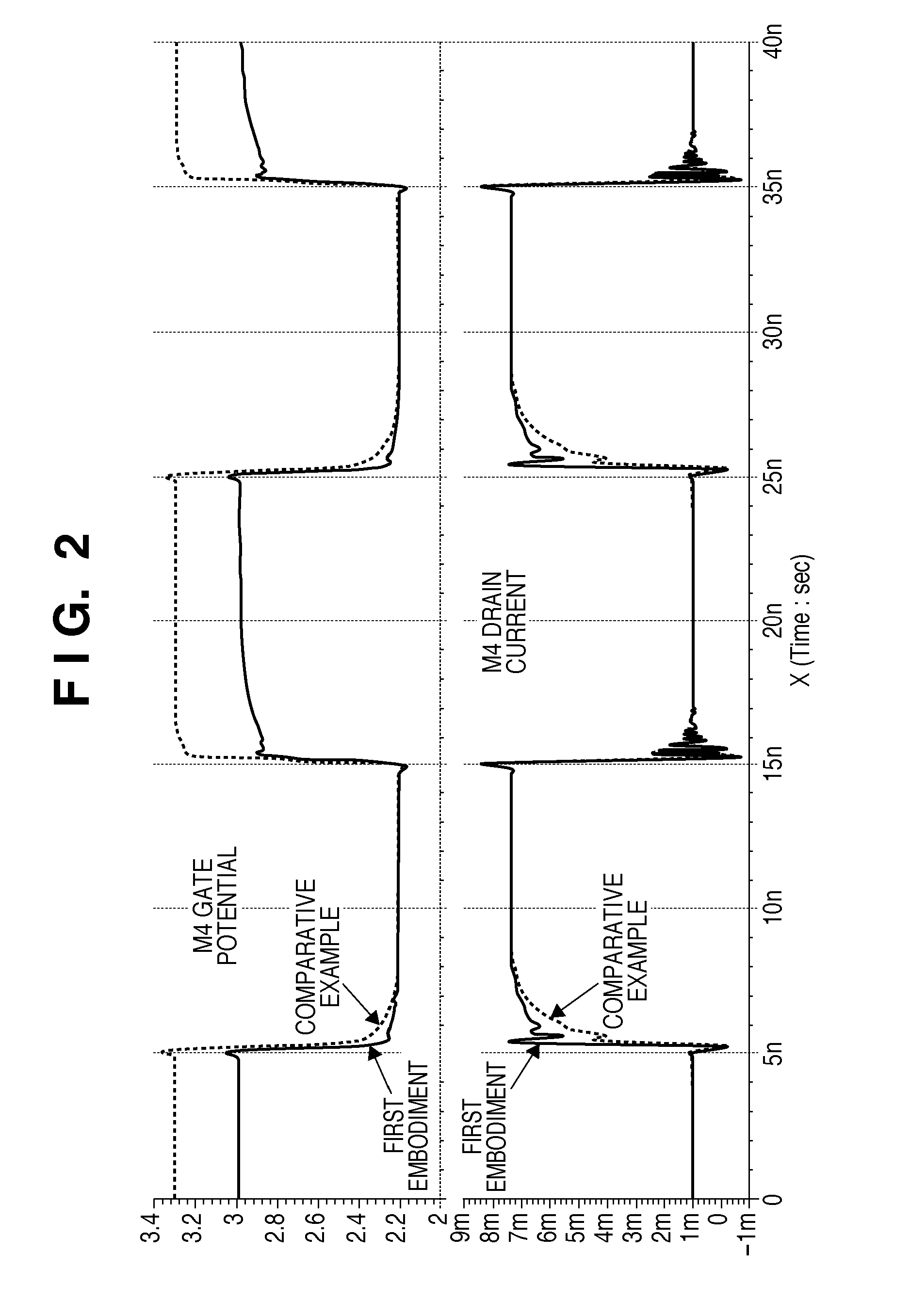
[0022]An example of a circuit arrangement according to the first embodiment will be described with reference to FIG. 1. Referring to FIG. 1, MOS transistors M1 and M4 constitute a current mirror circuit having a predetermined mirror ratio. The gate and drain of the MOS transistor M1 are connected to one terminal of a constant current source I1 whose other terminal is connected to GND (ground). The source of the MOS transistor M1 is connected to a power supply potential Vcc. The drain of a MOS transistor M2 is connected to both the gate and drain of the MOS transistor M1. The source of the MOS transistor M2 is connected to one terminal of a resistor R1 whose other terminal is connected to the gate of the MOS transistor M4. The source of the MOS transistor M2 is connected to one terminal of a resistor Rbias1 whose other terminal is connected to the drain of a MOS transistor M3. The source of the MOS transistor M2 is connected to one terminal of a constant current source Ibias whose ot...

second embodiment

[0026]An example of a circuit arrangement according to the second embodiment will be described with reference to FIG. 3. In FIG. 3, a potential to be supplied to the gate of a MOS transistor M4 is obtained by use of the following resistance circuit. This resistance circuit is formed by connecting a diode D in parallel with two serially connected resistors Rbias1 and Rbias2. The two resistors Rbias1 and Rbias2 divide the forward voltage for the diode D, which is generated by a constant current source Ibias, to obtain a potential to be supplied to the gate of a MOS transistor M4 from the connection point between the two resistors Rbias1 and Rbias2. Since other arrangements are the same as those in the first embodiment, a repetitive description of them will be omitted. In the second embodiment, the pre-bias voltage at the connection point between the two resistors Rbias1 and Rbias2 is given by Vbias=VF×{Rbias2 / (Rbias1+Rbias2)}, where VF represents the forward voltage of the diode. In t...

third embodiment

[0030]An example of a light emitting element driving circuit according to the third embodiment will be described with reference to FIG. 5. In FIG. 5, an LD is a light emitting element having current-current-to-light conversion characteristics. MOS transistors M1 and M4 constitute a current mirror circuit to operate this LD in accordance with differential data signals in a digital form.

[0031]The gate and drain of the MOS transistor M1 are connected to one terminal of a constant current source I1 whose other terminal is connected to a power supply Vcc. The source of the MOS transistor M1 is connected to GND (ground potential). MOS transistors M2 and M3 constitute a control block CTR BLOCK (control circuit) to ON / OFF-control the LD. The drain of the MOS transistor M2 is connected to both the gate and drain of the MOS transistor M1. The source of the MOS transistor M2 is connected to one terminal of a resistor R1 whose other terminal is connected to the gate of the MOS transistor M4, an...


PUM


Abstract

A light emitting element driving circuit for driving a light emitting element in accordance with a differential data signal for causing the light emitting element to turn on or turn off is provided. The circuit includes a first transistor, a first constant current source connected to a drain and gate of the first transistor and configured to supply a constant current through the drain and source of the first transistor, a second transistor configured to supply a certain current, and a control circuit configured to electrically connect or disconnect the gate of the first transistor to or from a gate of the second transistor via a first resistor. The control circuit may supply, to the gate of the second transistor, an intermediate potential in accordance with the other of the differential data signals, while the gate of the first transistor is electrically disconnected from the gate of the second transistor.

Description

BACKGROUND OF THE INVENTION[0001]1. Field of the Invention[0002]The present invention relates to a light emitting element driving circuit and, more particularly, to a light emitting element driving circuit for driving a light emitting element in a CMOS semiconductor integrated circuit used for image forming in a copy machine, laser beam printer (to be referred to as an LBP hereinafter), or the like which is required to operate with a low voltage, low driving current, and low cost.[0003]2. Description of the Related Art[0004]Conventionally, driving circuits for semiconductor light emitting elements have been devised to increase the pulse widths of output light signals from the semiconductor light emitting elements compared to the driving current pulse width. For example, the technique disclosed in Japanese Patent Laid-Open No. 05-152662 uses two stages of differential circuits and provides a level shift circuit between them. In addition, Japanese Patent Laid-Open No. 09-232635 disclo...

Claims


Application Information

Patent Timeline
Patent Type & Authority Patents(United States)
IPC IPC(8): H05B37/00
CPCH05B39/04Y02B20/14Y02B20/42Y02B20/00Y02B20/40G09G3/3283G09G2330/021
Inventor NAKAMURA, HIROYUKI
Owner CANON KK
Why Eureka
Try Eureka