Method of correcting a position of a prober

a prober and position correction technology, applied in the field of method of correcting the position of the prober, can solve problems such as electrical shorts between the pads, and achieve the effect of preventing electrical shorts

Inactive Publication Date: 2013-03-19
SAMSUNG ELECTRONICS CO LTD
View PDF16 Cites 0 Cited by
  • Summary
  • Abstract
  • Description
  • Claims
  • Application Information

AI Technical Summary

Benefits of technology

[0009]It is therefore a feature of an embodiment to provide a method of correcting a position of a prober that may be capable of preventing an electrical short between pads by a contact mark of the prober.

Problems solved by technology

Therefore, a contact mark of the needle, which may make contact with the boundary between the adjacent pads, may cause an electrical short between the pads.

Method used


Image

  • Method of correcting a position of a prober
  • Method of correcting a position of a prober
  • Method of correcting a position of a prober

Examples


Embodiment Construction

[0024]Korean Patent Application No. 10-2009-0008227, filed on Feb. 3, 2009, in the Korean Intellectual Property Office, and entitled: “Method of Correcting a Position of a Prober and Apparatus for Performing the Same,” is incorporated by reference herein in its entirety.

[0025]Example embodiments will now be described more fully hereinafter with reference to the accompanying drawings; however, they may be embodied in different forms and should not be construed as limited to the embodiments set forth herein. Rather, these embodiments are provided so that this disclosure will be thorough and complete, and will fully convey the scope of the invention to those skilled in the art. In the drawing figures, dimensions may be exaggerated for clarity of illustration. Like reference numerals refer to like elements throughout.

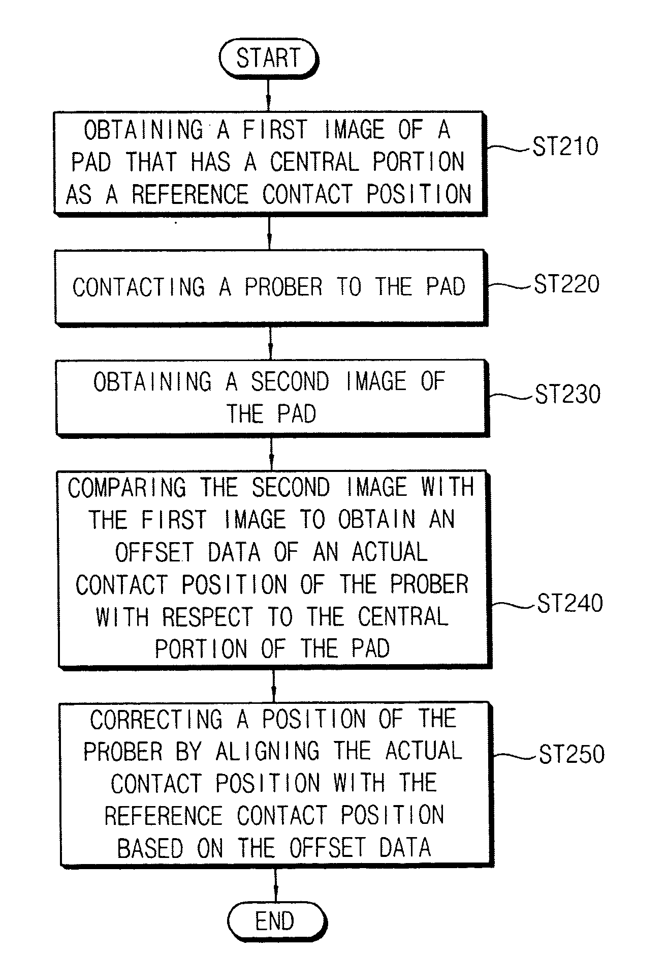
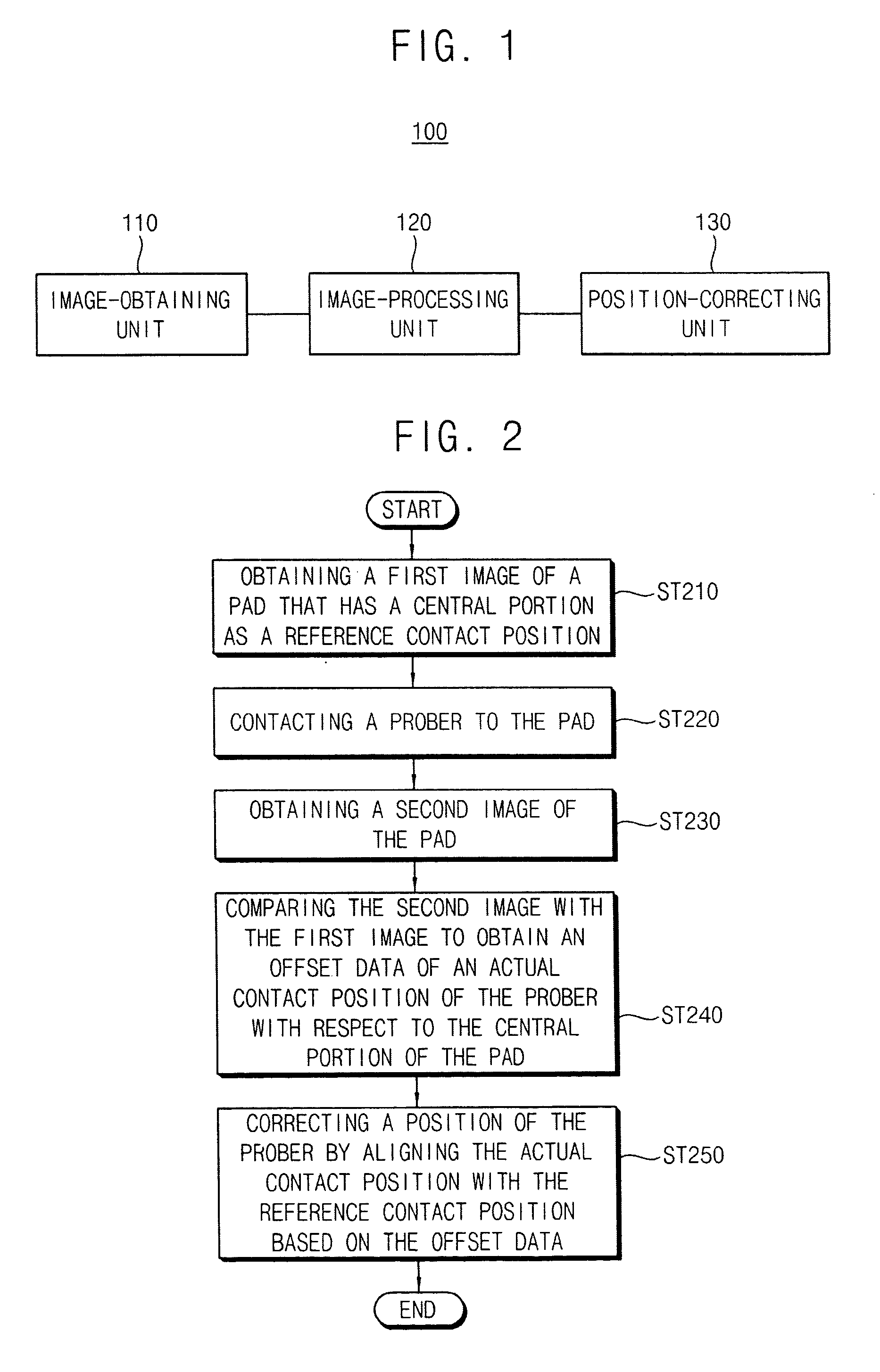
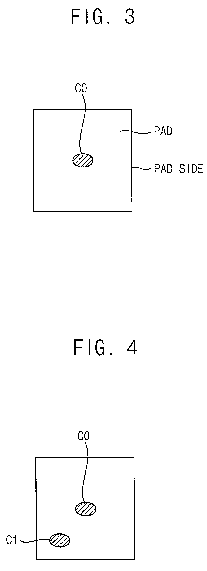
[0026]As set forth in detail below, example embodiments relate to a method of correcting a position of a prober used for inspecting a semiconductor device, and an apparatus...


PUM


Abstract

A method of correcting a position of a prober, the method including obtaining a first image of a pad, the pad having a predetermined reference contact position, contacting the prober to the pad after obtaining the first image of the pad, obtaining a second image of the pad after contacting the prober to the pad, determining an actual contact position of an actual contact mark on the pad, the actual contact mark being produced by the contacting of the prober to the pad, comparing the second image to the first image to obtain an offset data, the offset data relating the actual contact position to the reference contact position, and correcting the position of the prober by aligning the actual contact position with the reference contact position based on the offset data.

Description

BACKGROUND[0001]1. Field[0002]Example embodiments relate to a method of correcting a position of a prober and an apparatus for performing the same.[0003]2. Description of the Related Art[0004]Generally, a semiconductor device may be manufactured by performing a plurality of semiconductor fabrication processes on a semiconductor substrate. The semiconductor device may have pads as external terminals.[0005]A prober may be used for inspecting electrical characteristics of the semiconductor device. The prober may include a plurality of needles configured to make contact with the pads. The electrical characteristics of the semiconductor device may be inspected by contacting the needles to the pads.[0006]After contacting the needles to the pads, a contact mark may remain on the pad. When the needle does not make contact with a central portion of the pad, the contact mark may be connected with an adjacent pad, so that an electrical short between the pads may be generated.[0007]Further, as ...

Claims


Application Information

Patent Timeline
Patent Type & Authority Patents(United States)
IPC IPC(8): G01R31/00
CPCG01R31/2891H01L22/00
Inventor OH, SEUNG-YONGKIM, BYOUNG JOOCHI, DAE-GABKIM, KI-YOON
Owner SAMSUNG ELECTRONICS CO LTD
Why Eureka
Try Eureka