Method for fabricating semiconductor device

a semiconductor device and fuse technology, applied in semiconductor devices, semiconductor/solid-state device details, electrical equipment, etc., can solve the problems of difficult control of the insulation layer, difficult to cut the fuse, and excessive time for repair-etching, so as to prevent an electrical short

Active Publication Date: 2008-09-11
SK HYNIX INC
View PDF7 Cites 0 Cited by
  • Summary
  • Abstract
  • Description
  • Claims
  • Application Information

AI Technical Summary

Benefits of technology

[0017]Embodiments of the present invention are directed to providing a method for fabricating a semiconductor device, c

Problems solved by technology

For this reason, during the repair-etching, it takes excessive time to perform the repair-etching, and it is difficult to control the insulation layer 15 having a predetermined thickness so as to be formed over the fuse at a uniform thickness.
Thus, when laser fuse cutting is subsequently performed, points between the respective layers, reacting with laser power, are different from each other, so that it is difficult to cut the fuse.
Further, after the laser fuse cutting, cr

Method used


Image

  • Method for fabricating semiconductor device
  • Method for fabricating semiconductor device
  • Method for fabricating semiconductor device

Examples


Embodiment Construction

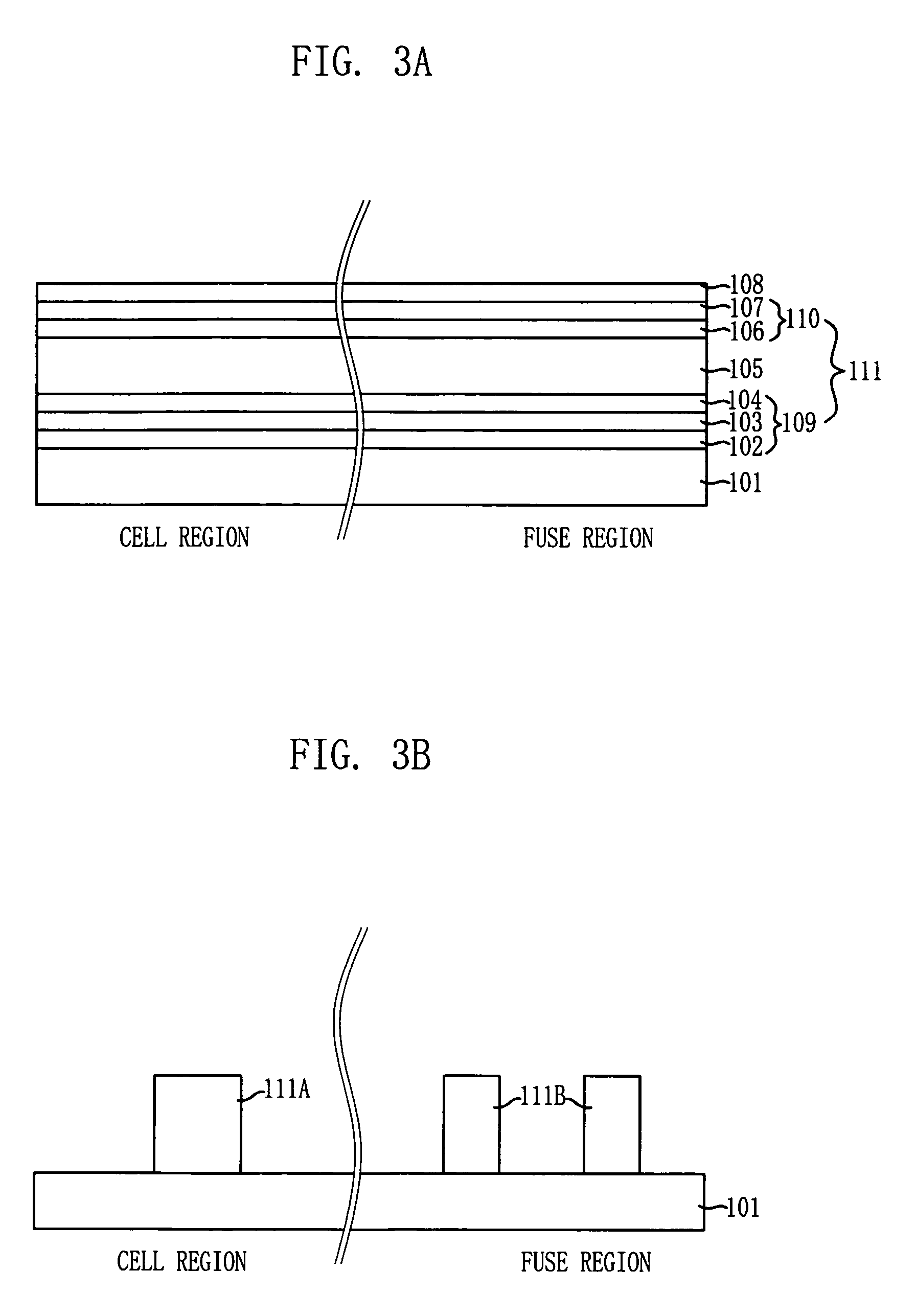
[0021]FIGS. 3A to 3E are cross-sectional views of a method for fabricating a semiconductor device in accordance with an embodiment of the present invention.

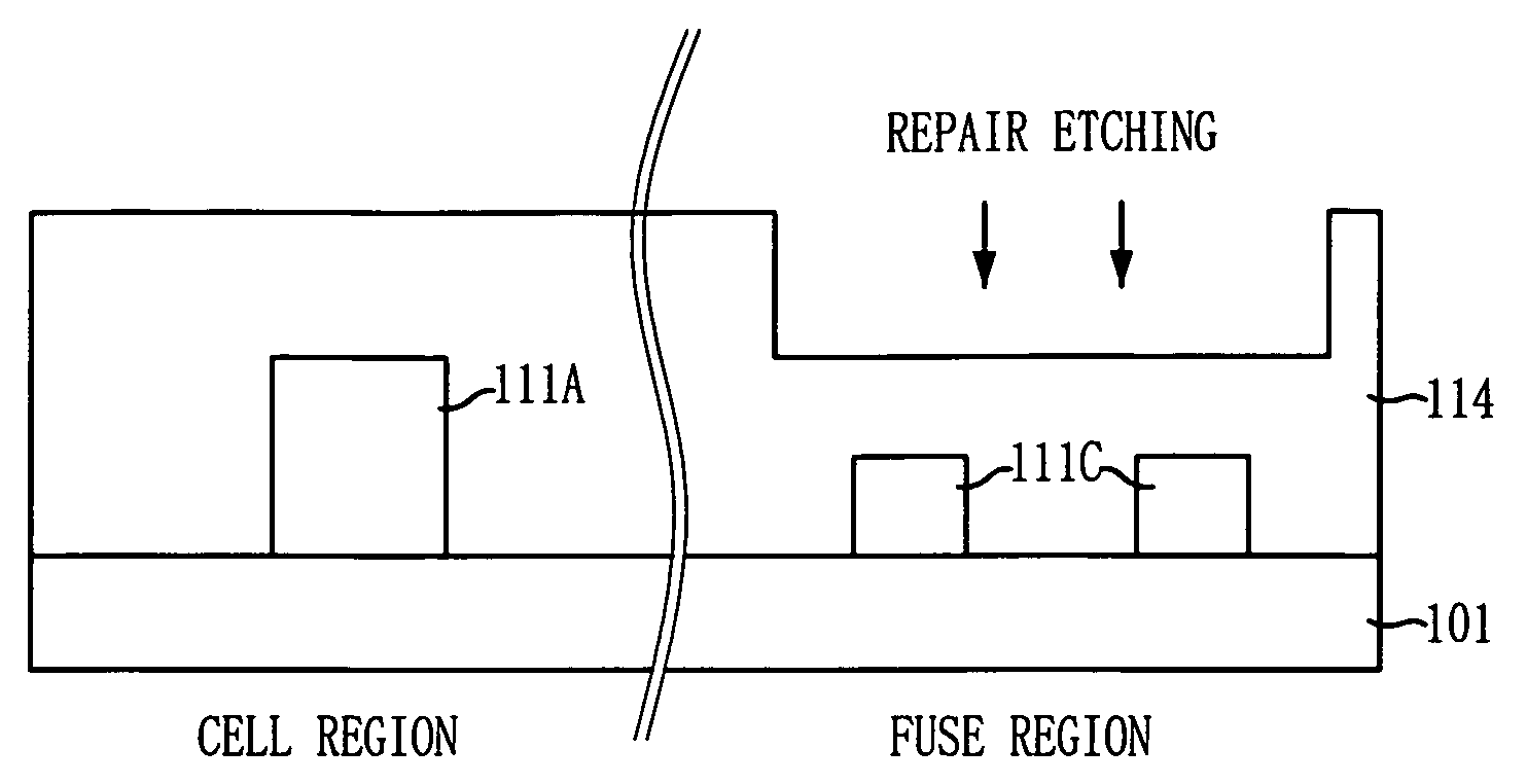
[0022]Referring to FIG. 3A, an interconnection layer 111 is formed over a substrate 101 having a cell region and a fuse region. Here, the substrate 101 may be a substrate on which a dynamic random access memory (DRAM) process is performed, or a substrate in which some processes of forming, for instance, a gate pattern, a bit line pattern, a capacitor, and an interlayer insulation layer are completed before the interconnection layer 111 is formed. Further, the interconnection layer 111 is formed in the cell and fuse regions at the same time, and is used as a metal interconnection in the cell region and as one fuse in the fuse region through a subsequent patterning process.

[0023]Particularly, the interconnection layer 111 is formed in a stacked structure in which a barrier layer 109, metal layers 105 and 105A, and an anti-reflectiv...


PUM


Abstract

A method for fabricating a semiconductor device includes forming a fuse over a substrate, the fuse having a barrier layer, a metal layer, and an anti-reflective layer stacked, selectively removing the anti-reflective layer, forming an insulation layer over a whole surface of the resultant structure including the fuse, and performing repair-etching such that part of the insulation layer remains above the fuse.

Description

CROSS-REFERENCE TO RELATED APPLICATIONS[0001]The present invention claims priority of Korean patent application number 2007-0021453, filed on Mar. 5, 2007, which is incorporated by reference in its entirety.BACKGROUND OF THE INVENTION[0002]The present invention relates to a method for fabricating a semiconductor device and, more particularly, to a method of forming a fuse for a semiconductor device.[0003]When a failure occurs in a semiconductor device, a fuse is used to repair such a failed part. In other words, in the case in which such a fail is neither a hard fail nor a severe fail after a semiconductor fabrication process is completed, a fuse line, that is a redundancy line, is cut off using a laser. Thereby, the operation of the semiconductor device is made possible.[0004]Up to now, the fuse is not separately formed by an additional process, but is formed by using a conductive layer made up of a bit line, a word line, or the plate line (upper electrode) of a capacitor.[0005]FIG...

Claims


Application Information

Patent Timeline
IPC IPC(8): H01L21/02
CPCH01L23/5258H01L2924/0002H01L2924/00H01L21/82H01L23/62
Inventor PARK, HYUN-SIKLEE, HAE-JUNGLEE, JAE-KYUN
Owner SK HYNIX INC
Why Eureka
Try Eureka