Packaging a semiconductor device having wires with polymerized insulator skin

a technology of polymerized insulator skin and semiconductor devices, applied in the direction of plastic/resin/waxes insulators, basic electric elements, coatings, etc., can solve the problems of limiting the density of bonded wires, electrical shorts and device malfunction, and difficulty in forming free air balls, ball bonds, and stitch bonds, etc., to prevent electrical shorts, additional time, equipment or expenditure

Active Publication Date: 2015-02-05
TEXAS INSTR INC
View PDF5 Cites 2 Cited by
  • Summary
  • Abstract
  • Description
  • Claims
  • Application Information

AI Technical Summary

Benefits of technology

[0010]It is a technical advantage of the invention that the method for forming the insulating skin covering the wires and preventing an electrical short does not require additional time, equipment or expenditure compared to conventional wire bonding and encapsulation processes.
[0011]It is another technical advantage that the method of the invention can be implemented in any packaging process flow of any semiconductor device using wire bonding and plastic encapsulation.

Problems solved by technology

As a consequence, a major factor limiting the density of bonded wires is wire sweep during the molding processes for creating the plastic encapsulation.
Wire sweep not only distorts the configurations and orderly sequence of wire spans, but it may result in mutual touching of adjacent wires, which causes electrical shorts and device malfunctioning.
Another method for reducing wire sweep proposes the use of wires in insulating tubes or pipes; this approach, however, was found to cause difficulties in forming free air balls, ball bonds, and stitch bonds, and in contaminating capillaries.
It turned out that this approach of direct coating with an insulating polymeric compound may cause mismatch of the coefficients of thermal expansion between dispensed polymers and molding compounds with the conventional >85 weight % inorganic fillers.

Method used


Image

  • Packaging a semiconductor device having wires with polymerized insulator skin
  • Packaging a semiconductor device having wires with polymerized insulator skin
  • Packaging a semiconductor device having wires with polymerized insulator skin

Examples


Embodiment Construction

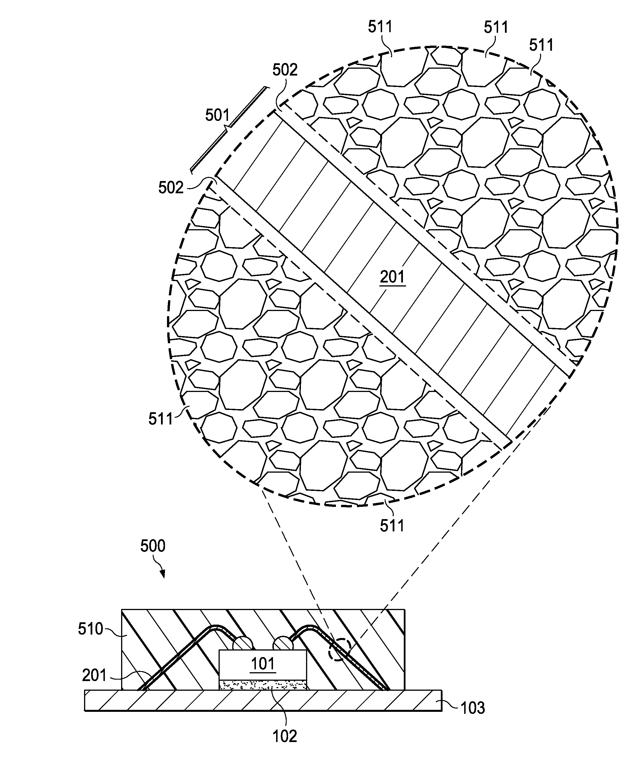
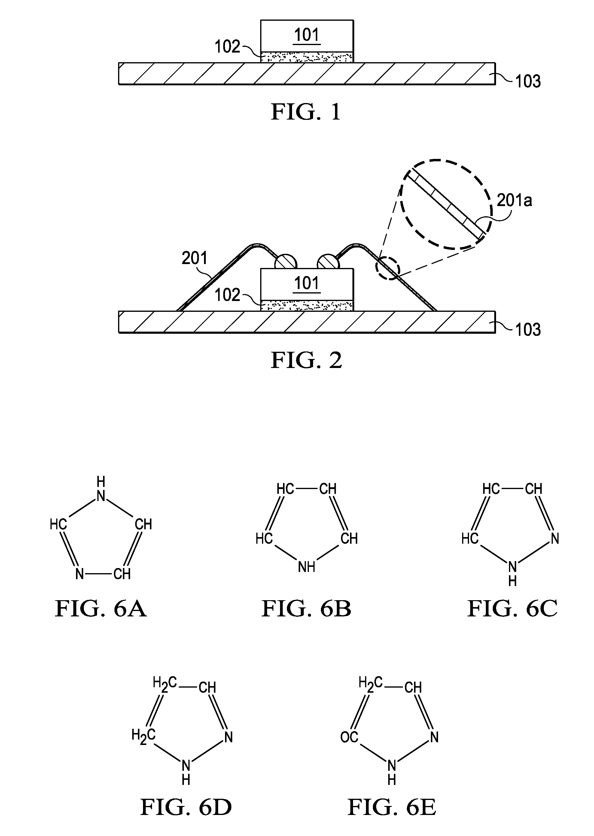
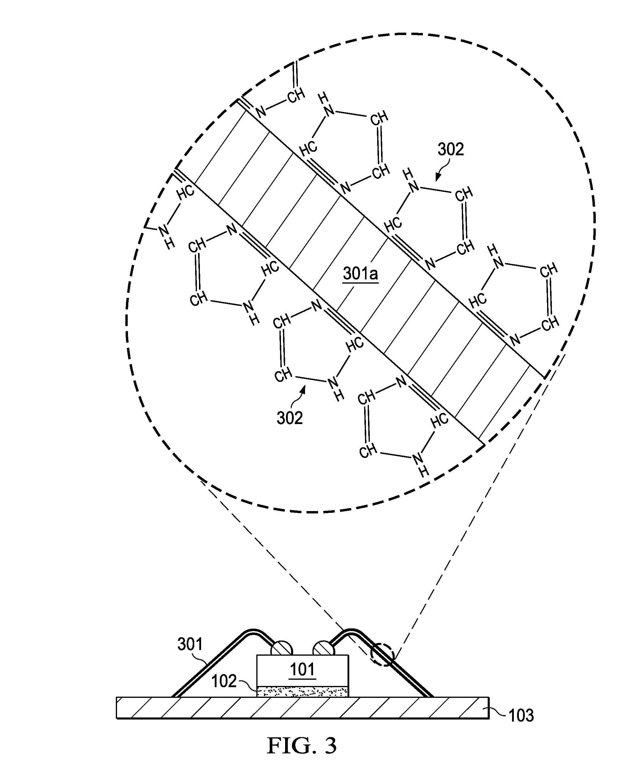
[0024]An embodiment of the invention is a method for fabricating a plastic encapsulated semiconductor device with bonding wires, which are protected against electrical shorting if they should touch due to wire sweep during the encapsulation process. FIGS. 1 to 5 illustrate certain steps of the fabrication method using an exemplary device for demonstration. In FIG. 1, a semiconductor chip 101 is attached with an adhesive layer 102 to a substrate 103. Chip 101 has a plurality of bondable terminal pads. Chip 101 may be made of silicon, silicon germanium, gallium arsenide, III-V compounds, or any other material used in electronic technology. The terminal pads may be metal such as aluminum or copper, or any other material onto which conductive connectors can be affixed. Substrate 103 may be a metal leadframe or a multimetal-level substrate, laminated substrate, or any other suitable support structure.

[0025]FIG. 2 depicts the process step of attaching bonding wires 201 to the chip termina...


PUM

PropertyMeasurementUnit
liquefying temperatureaaaaaaaaaa
diameteraaaaaaaaaa
diameteraaaaaaaaaa

Abstract

A chip is attached to a substrate with wires spanning from the chip to the substrate is loaded in a heated cavity of a mold. The wire surfaces are coated with an adsorbed layer of molecules of a heterocyclic compound. A pressure chamber of the mold is loaded with a solid pellet of a packaging material including a polymerizable resin. The chamber is connected to the cavity. The vapor of resin molecules is allowed to spread from the chamber to the assembly inside the cavity during the time interval needed to heat the solid pellet for rendering it semi-liquid and to pressurize it through runners before filling the mold cavity, wherein the resin molecules arriving in the cavity are cross-linked by the adsorbed heterocyclic compound molecules into an electrically insulating at least one monolayer of polymeric structures on the wire surfaces.

Description

CROSS REFERENCE TO RELATED APPLICATIONS[0001]This application is a Divisional of and claims priority to U.S. patent application Ser. No. 13 / 787,198 filed 03 / 06 / 2013, which claims the benefit of Provisional Application Ser. No. 61 / 625,996 filed Apr. 18, 2012. Said applications are hereby incorporated by reference herein in their entirety.FIELD[0002]The embodiments of the invention are related in general to the field of semiconductor devices and processes, and more specifically to plastic-packaged semiconductor devices with bonding wires having wire short protection by a polymerized insulator skin around the wires, and methods to fabricate these protections.DESCRIPTION OF RELATED ART[0003]The ongoing trend towards miniaturization, high performance and cost reduction of plastic packaged semiconductor devices drives ever higher density of the wire bonds employed for these packages. The required wire density, in turn, drives not only a reduction of the pitches of the bond pads, for insta...

Claims


Application Information

Patent Timeline
Patent Type & Authority Applications(United States)
IPC IPC(8): H01L21/56H01L23/00H01L23/29
CPCH01L21/56H01L23/295H01L2924/0665H01L2224/4382H01L24/43B29C45/0001B29C45/0046B29C45/14655B29C45/14836H01B3/40H01L21/565H01L24/05H01L24/29H01L24/32H01L24/45H01L24/48H01L24/85H01L2224/04042H01L2224/05624H01L2224/05647H01L2224/2919H01L2224/32225H01L2224/32245H01L2224/43848H01L2224/45014H01L2224/45015H01L2224/45124H01L2224/45144H01L2224/45147H01L2224/48091H01L2224/48227H01L2224/48247H01L2224/48463H01L2224/48465H01L2224/48624H01L2224/48647H01L2224/48724H01L2224/48747H01L2224/48824H01L2224/48847H01L2224/73265H01L2224/8592H01L2224/92247H01L2924/00014H01L2924/10253H01L2924/10271H01L2924/1032H01L2924/10329H01L2924/181H01L2924/3862H01L2924/20752H01L2924/078H01L2924/00H01L2924/00012H01L2924/206C08K3/10C08K3/36C08K7/14H01L23/4952H01L2224/48221H01L2224/485
Inventor ZHANG, RONGWEICASTRO, ABRAM
Owner TEXAS INSTR INC
Why Eureka
Try Eureka