
Organic light-emitting display device having improved transmittance

a display device and organic technology, applied in the direction of semiconductor devices, basic electric elements, electrical equipment, etc., can solve the problems of significant voltage drop and image distortion of the user's view, and achieve the effect of preventing or reducing the distortion of the image transmitted, preventing or reducing the transmission of ligh

Active Publication Date: 2013-10-29
SAMSUNG DISPLAY CO LTD
View PDF23 Cites 3 Cited by
  • Summary
  • Abstract
  • Description
  • Claims
  • Application Information

AI Technical Summary

Benefits of technology

[0011]Aspects of embodiments according to the present invention are directed toward a transparent organic light-emitting display device having an improved transmittance and a reduced voltage drop in an opposite electrode.
[0012]Aspects of embodiments according to the present invention are also directed toward a transparent organic light-emitting display device that prevents or reduces distortion of an image transmitted therethrough by preventing or reducing light transmitting therethrough from scattering.

Problems solved by technology

Also, an image viewable to the user may be distorted due to the above-described patterns, i.e., the patterns of the organic light-emitting devices, the thin film transistors, and the wires.
Furthermore, when an opposite electrode to be commonly deposited on the entire screen is formed with a small thickness in order to improve the transmittance of external light, a voltage drop, i.e., an IR drop, may occur at the opposite electrode, and in particular, as the size of an organic light-emitting display device is increased, the voltage drop may be significant.

Method used


Image

  • Organic light-emitting display device having improved transmittance
  • Organic light-emitting display device having improved transmittance
  • Organic light-emitting display device having improved transmittance

Examples


Embodiment Construction

[0047]The present invention will now be described more fully with reference to the accompanying drawings in which exemplary embodiments of the invention are shown.

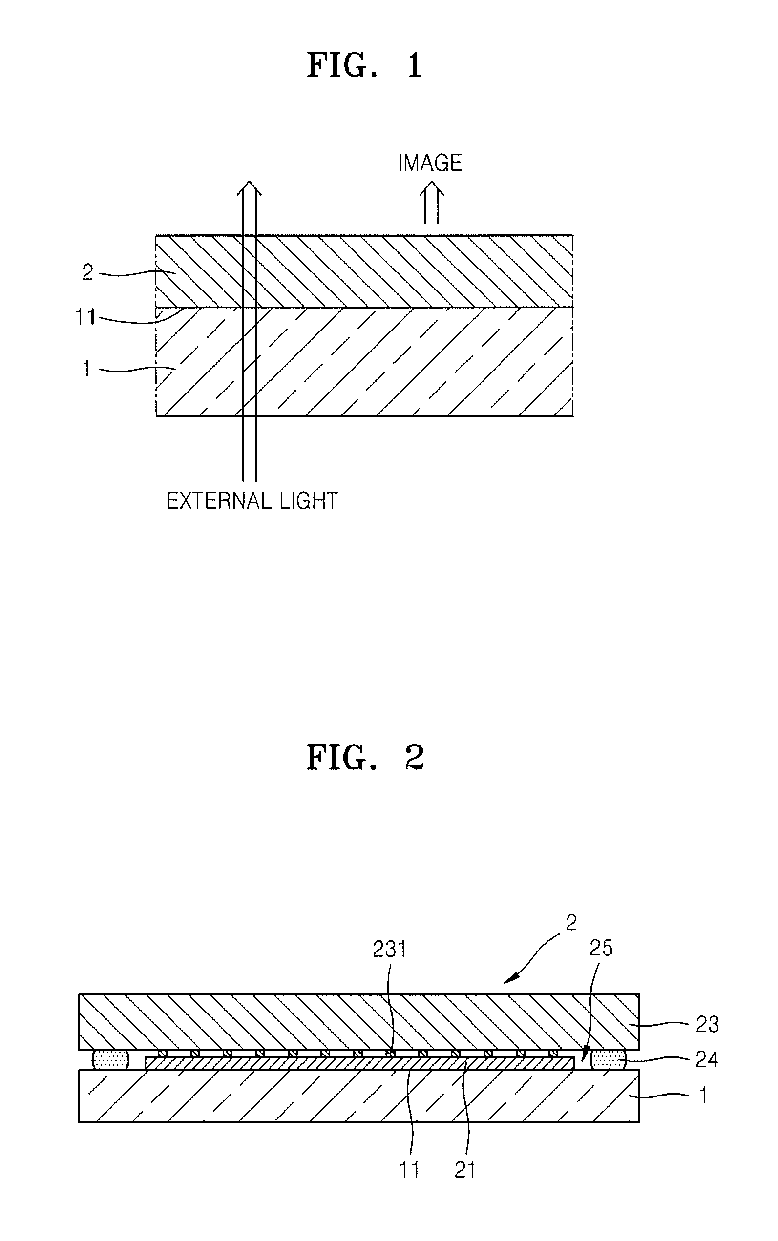
[0048]FIG. 1 is a cross-sectional view of an organic light-emitting display device according to an embodiment of the present invention.

[0049]Referring to FIG. 1, the organic light-emitting display device according to an embodiment of the present invention includes a display unit 2 formed on a first surface 11 of a first substrate 1.

[0050]In the organic light-emitting display device, external light enters through the first substrate 1 and the display unit 2.

[0051]As will be described in more detail later, the display unit 2 is formed to allow external light to transmit therethrough. That is, referring to FIG. 1, the display unit 2 is formed in such a way that a user at a side where an image is displayed can observe an external image through the first substrate 1.

[0052]FIG. 2 is an enlarged cross-sectional view specifically ...


PUM


Abstract

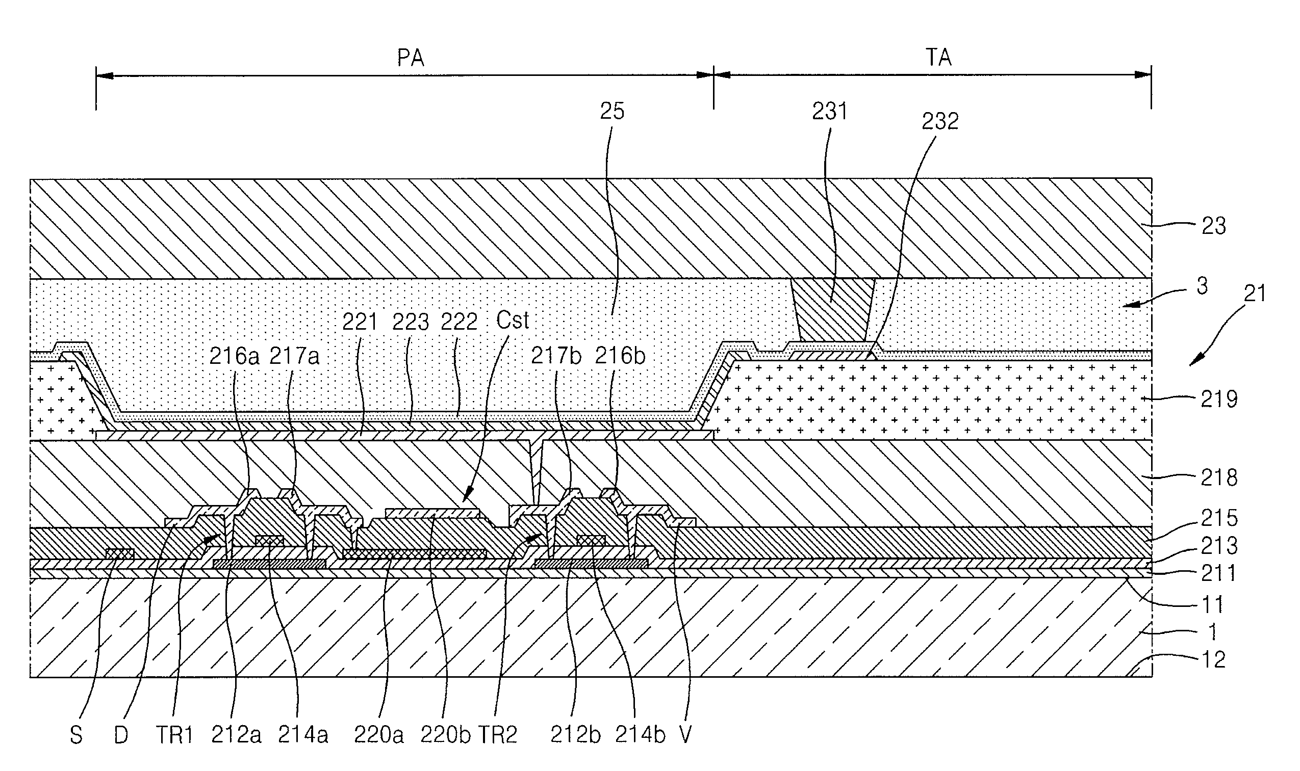
A transparent organic light-emitting display device has an improved transmittance and a reduced voltage drop in an opposite electrode. The organic light-emitting display device includes: a first substrate having a transmitting region and a plurality of pixel regions separated from each other by the transmitting region interposed between the pixel regions; a plurality of pixel electrodes being located at the pixel regions, respectively; an opposite electrode facing the pixel electrodes and being at the transmitting region and the pixel regions; a second substrate facing the opposite electrode and being bonded to the first substrate; a first conductive unit being between the second substrate and the opposite electrode, opposite ends of the first conductive unit contacting the second substrate and the opposite electrode, respectively; and a second conductive unit facing the first conductive unit and contacting the opposite electrode that is between the first conductive unit and the second conductive unit.

Description

CROSS-REFERENCE TO RELATED PATENT APPLICATION[0001]This application claims priority to and the benefit of Korean Patent Application No. 10-2010-0063868, filed on Jul. 2, 2010, in the Korean Intellectual Property Office, the disclosure of which is incorporated herein in its entirety by reference.BACKGROUND[0002]1. Field[0003]Aspects of embodiments according to the present invention relate to an organic light-emitting display device, and more particularly, to a transparent organic light-emitting display device.[0004]2. Description of the Related Art[0005]Applications of organic light-emitting display devices range from personal portable devices, such as MP3 players and mobile phones, to television sets due to having superior characteristics such as wide viewing angles, high contrast ratios, fast response times, and low power consumption.[0006]An organic light-emitting display device has self light-emitting characteristics, and the weight and thickness of the organic light-emitting dis...

Claims


Application Information

Patent Timeline
Patent Type & Authority Patents(United States)
IPC IPC(8): H01L29/04
CPCH01L27/3279H01L51/5228H01L27/326H01L51/524H10K59/121H10K59/1315H10K50/824H10K50/841
Inventor HA, JAE-HEUNGHWANG, KYU-HWANYOON, SEOK-GYUSONG, YOUNG-WOOLEE, JONG-HYUKKIM, KEUM-NAMHWANG, YOUNG-IN
Owner SAMSUNG DISPLAY CO LTD
Learn More