High frequency semiconductor switch

a high-frequency semiconductor and switch technology, applied in the direction of semiconductor devices, electrical equipment, transistors, etc., can solve the problems of insufficient voltage distribution, deterioration and inability to obtain adequate voltage distribution, so as to improve improve the effect of insertion loss characteristics and harmonic characteristics

Active Publication Date: 2014-03-18
SAMSUNG ELECTRO MECHANICS CO LTD
View PDF4 Cites 2 Cited by
  • Summary
  • Abstract
  • Description
  • Claims
  • Application Information

AI Technical Summary

Benefits of technology

[0008]An aspect of the present invention provides a high frequency semiconductor switch capable of improving insertion loss characteristics and harmonic characteristics by allowing for good voltage distribution in a gate wiring.
[0010]According to the configuration, the parallel portion is formed with two ends and the path applying voltage from the gate via is divided. Therefore, the embodiments of the present invention can reduce voltage drop due to a length of a path being short, thereby allowing voltage distribution to be more uniform.

Problems solved by technology

In this case, voltage may fall due to a resistance component of the lengthwise extended gate and as a result, adequate voltage distribution may not be obtained.
As a result, insertion loss characteristics and harmonic characteristics may be deteriorated.

Method used


Image

  • High frequency semiconductor switch
  • High frequency semiconductor switch
  • High frequency semiconductor switch

Examples


first embodiment

(First Embodiment)

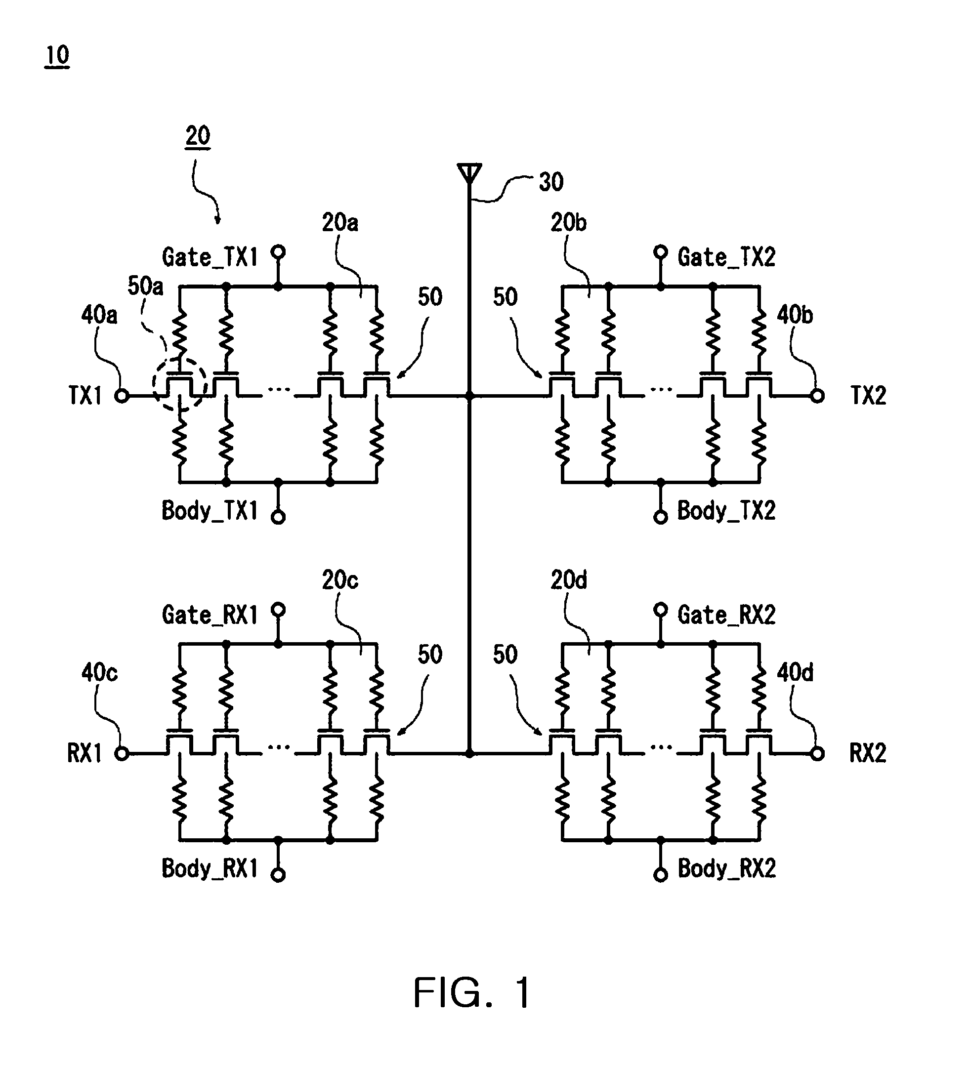
[0024]FIG. 1 is a diagram showing an example of a schematic circuit configuration of a high frequency semiconductor switch according to a first embodiment of the present invention.

[0025]As shown in FIG. 1, a high frequency semiconductor switch 10 may include four series switches 20a to 20d. The series switches 20a to 20d may be disposed between an antenna terminal 30 and RF terminals 40a to 40d. The series switches 20a to 20d may each include at least one field effect transistor (hereinafter, referred to as FET). As shown in FIG. 1, gates of a plurality of FETs included in the same series switches 20a to 20d may simultaneously receive voltage applied thereto. Therefore, conduction between the antenna terminal 30 and the RF terminals 40a to 40d may be controlled by switching voltage applied to the gates for each series switch, 20a to 20d. Alternatively, a body of the FET may also have voltage applied thereto.

[0026]In an example shown in FIG. 1, in the RF terminals 4...

second embodiment

(Second Embodiment)

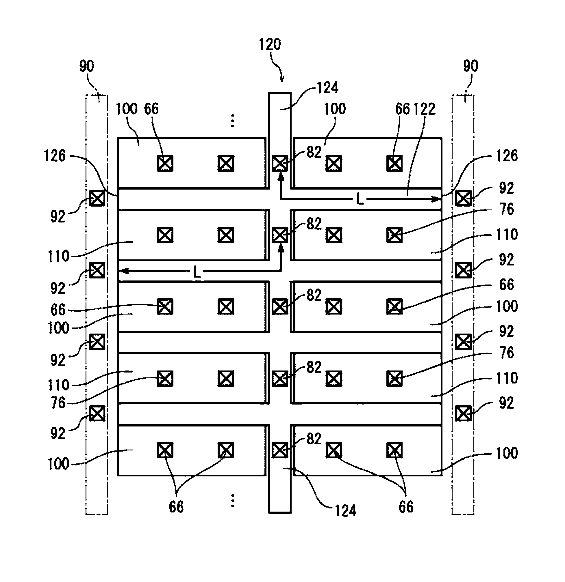
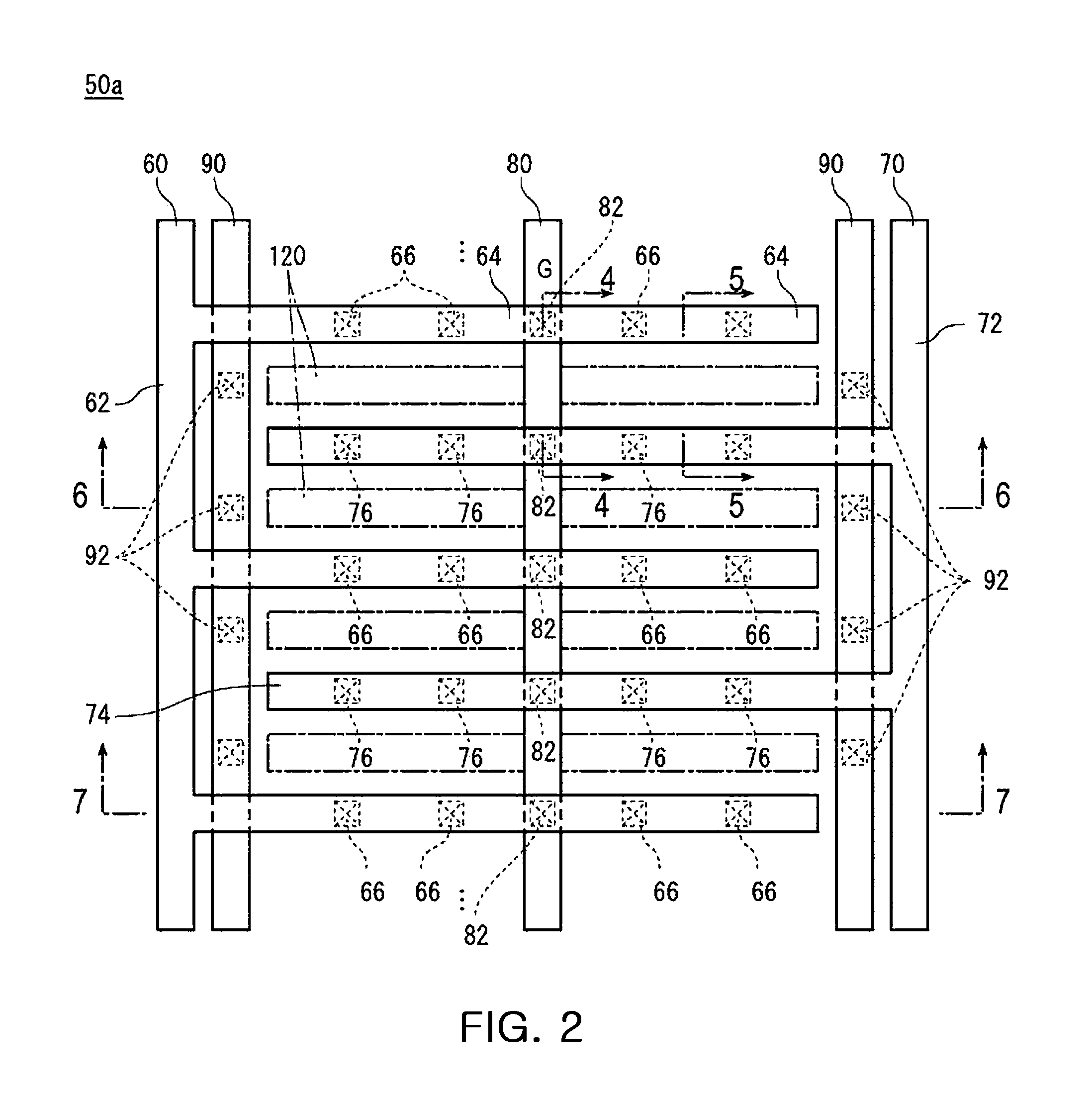
[0051]FIG. 9 is a schematic plan view showing gate, source, drain wirings of an FET included in a high frequency semiconductor switch according to a second embodiment of the present invention, FIG. 10 is a schematic plan view showing gate, source, drain wirings disposed under the wiring according to the second embodiment of the present invention, and FIG. 11 is a schematic cross-sectional view of the FET taken along line 11-11 of FIG. 9. The same components as those of the first embodiment of the present invention are denoted by the same reference numerals and the description thereof will be omitted.

[0052]In the FET 50 included in the high frequency semiconductor switch according to the second embodiment of the present invention, a source wiring 260 and a drain wiring 270 may be formed in a comb type similar to the first embodiment of the present invention. The source wiring 260 and the drain wiring 270 may respectively include stem portions 262 and 272, teeth por...


PUM


Abstract

There is provided a high frequency semiconductor switch for improving insertion loss characteristics and harmonic characteristics by providing good voltage distribution in a gate wiring. The field effect transistor includes a source wiring electrically connected to a source region formed on a substrate and extending unidirectionally; a drain wiring electrically connected to a drain region formed on the substrate and extending in parallel with the source wiring; a gate having a parallel portion extending between the source wiring and the drain wiring in approximately parallel with the source wiring and the drain wiring; a gate wiring applying voltage to the gate; and a gate via electrically connecting the gate to the gate wiring, the parallel portion including two ends and formed with a path applying voltage to each of the two ends from the gate via.

Description

BACKGROUND OF THE INVENTION[0001]1. Field of the Invention[0002]The present invention relates to a high frequency semiconductor switch, and more particularly, to a high frequency semiconductor switch used in wireless communications apparatuses.[0003]2. Description of the Related Art[0004]A front end of wireless communications apparatuses such as mobile phones, PCs, and the like, has had a high frequency semiconductor switch mounted therein. The high frequency semiconductor switch switches a path along which a signal received from an antenna is transferred and a path along which a signal transmitted from the antenna is transferred. To facilitate switching, the high frequency semiconductor switch includes a plurality of field effect transistors (FETs).[0005]The FETs are connected to a transmission terminal to which a transmission signal is input, or a reception terminal from which a receiving signal is output. When a signal is transmitted, voltage is applied to a gate of the FET conne...

Claims


Application Information

Patent Timeline
Patent Type & Authority Patents(United States)
IPC IPC(8): H01L29/76
CPCH01L27/1203H01L29/41758
Inventor SUGIURA, TSUYOSHI
Owner SAMSUNG ELECTRO MECHANICS CO LTD
Why Eureka
Try Eureka