Image pickup device and method for manufacturing the image pickup device

a pickup device and pickup device technology, applied in the field of image pickup device and a manufacturing method of image pickup device, can solve the problems of deteriorating the cutting blade for dicing, reducing productivity, and difficult to cut precisely enough to maintain high optical performance, and achieves high productivity, high cutting resistance, and high optical performance.

Inactive Publication Date: 2014-07-29
KONICA MINOLTA OPTO
View PDF17 Cites 7 Cited by
  • Summary
  • Abstract
  • Description
  • Claims
  • Application Information

AI Technical Summary

Benefits of technology

[0053]According to the present invention, in spite of employing a configuration of a plurality of laminated wafer lenses, there is no need for bonding the first lens block and the second lens block through a separate spacer such as a glass substrate, whereby cutting resistance when cutting does not needs to be increased, thereby maintaining a high productivity due to using wafer lenses.
[0054]In addition, it can also solve the problem that the optical performance is adversely affected by misalignment of the optical axes caused by a positional displacement between the wafer lenses to be bonded to other members when they are cut.
[0055]In addition, as a result of removing spacers between lenses, it becomes to be possible to cut the optical system including a spacer necessary between an image sensor and an optical system, whereby design can be done, allowing the material and the allowance of the thickness of the spacer to have degree of freedom; thus the lens unit made by cutting together with the spacer into individual pieces is bonded to a sensor unit made by cutting another wafer into individual pieces, forming a step in a side surface, and the lens block is covered by a package so that the lens block is housed in that step, whereby the lens block does not stick out of the sensor unit, with a result that a small-sized and high performance image pickup device can be provided.

Problems solved by technology

Such wafer lenses are advantageous in that by using these lenses, image pickup devices, especially small optical systems such as a camera for a portable phone, can be produced in one shot; however, they have some issues.
However, in the method of cutting a plurality of wafer lenses which are laminated, there arise the following technical problems: there are a lot of glass substrates therebetween; there are a lot of intervening members such as spacers defining spaces between the lens parts such as a spacer defining the space to the image sensor for receiving light from the lens; and the cut resistance when cutting is accordingly increased, thereby deteriorating the cutting blade for dicing and the like, whereby the productivity is decreased, and thus it is difficult to cut precisely enough to maintain high optical performance.

Method used


Image

  • Image pickup device and method for manufacturing the image pickup device
  • Image pickup device and method for manufacturing the image pickup device
  • Image pickup device and method for manufacturing the image pickup device

Examples


first embodiment

[0146][Image Pickup Device]

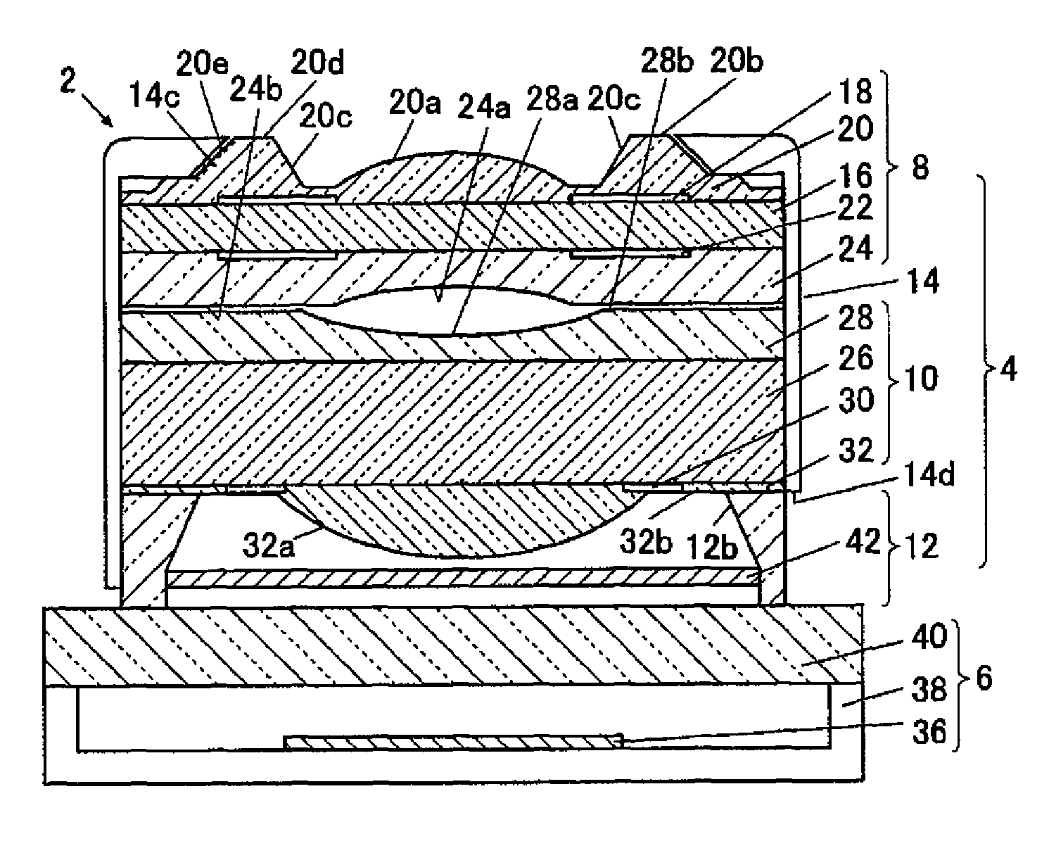
[0147]As shown in FIG. 1a, an image pickup device 2 is mainly constituted by a lens unit 4 and a sensor unit 6, and the lens unit 4 is disposed on the sensor unit 6. The sensor unit 6 has a larger area than the lens unit 4, and thus the lens unit 4 is mounted on the center of the sensor unit 6 with an open area (forming a step) on the circumference of the sensor unit 6.

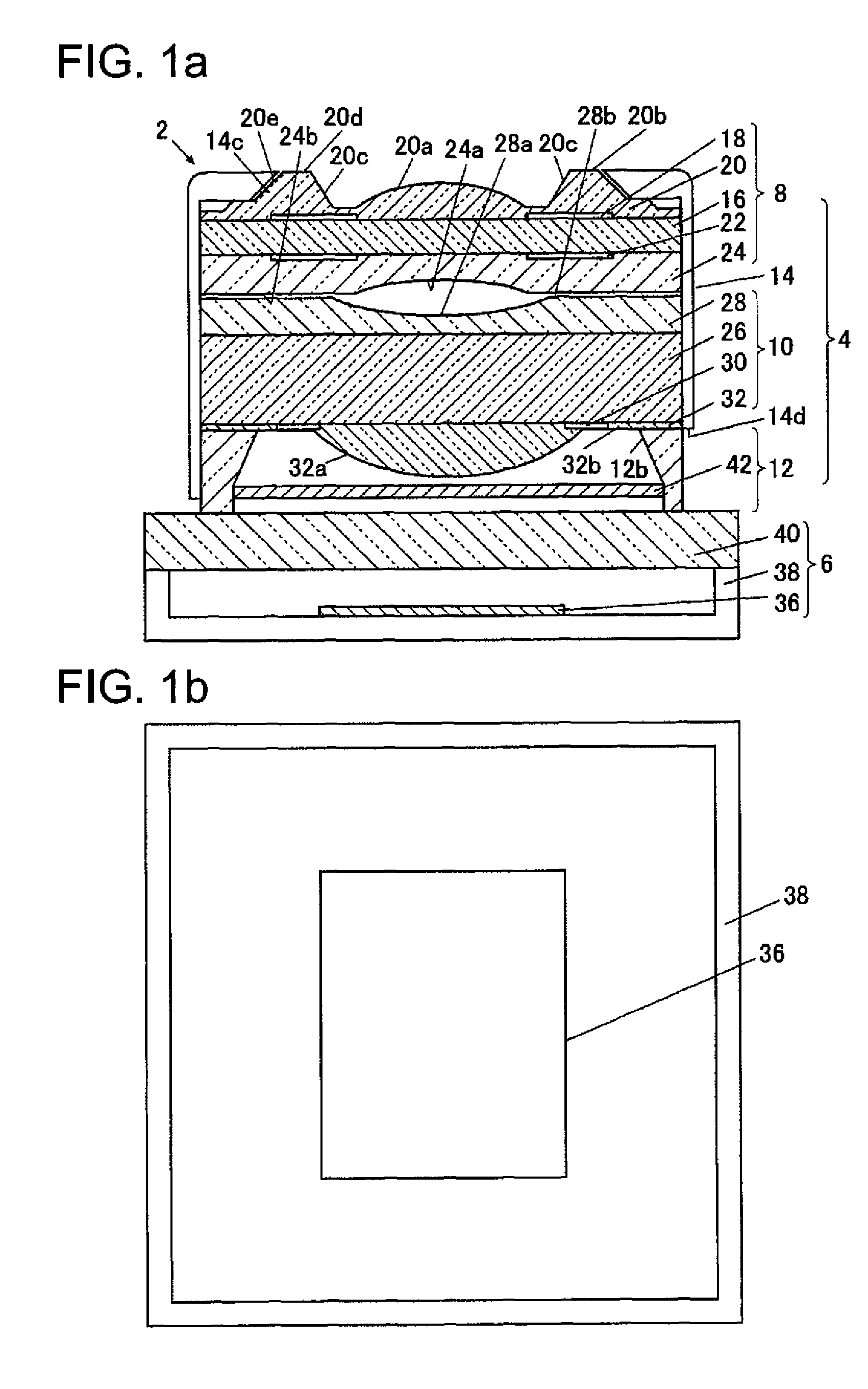
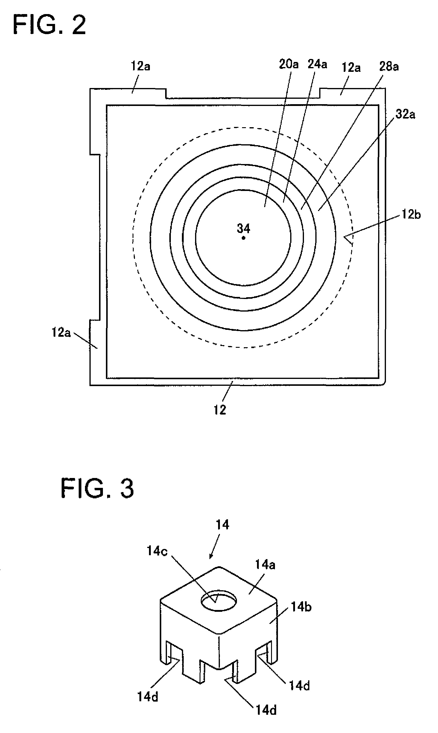
[0148]The lens unit 4 includes: a lens block 8 in which a convex lens part 20a, a glass substrate 16, and a concave lens part 24a are bonded together; a lens block 10 in which a concave lens part 28a, a glass substrate 26, and a convex lens part 32a are bonded together; a spacer 12; and a covering package 14, wherein the lens blocks 8 and 10 and the spacer 12 are stacked and bonded and covered by a covering package 14.

[0149]The lens block 8 has a plate-like glass substrate 16. On the glass substrate 16, there are formed an aperture stop 18 and a resin part 20, and under the glass substrate 1...

second embodiment

[0576]The second embodiment is different from the first embodiment mainly on the following points, but the same as the first embodiment on the other points.

[0577]As a wafer lens manufacturing apparatus, instead of the wafer lens manufacturing apparatus 300, a wafer lens manufacturing apparatus 700 is used.

[0578]In producing the wafer lens 52 or 54, instead of a so-called step-and-repeat method (a method in which a molding die 450 is relatively moved to produce convex lens parts 20a and the like, gradually), a so-called batch method (a method in which a molding die 770 is pressed on a glass substrates 16 and 26 once to collectively produce the convex lens parts 20a and the like) is employed.

[0579][Wafer Lens Manufacturing Apparatus (Batch Method)]

[0580]As shown in FIG. 68, the wafer lens manufacturing apparatus 700 has a base 702.

[0581]On the upper part of the base 702, there is formed an opening section 704. Over the opening section 704, there is provided a plate-like lid body 706 d...


PUM


Abstract

Disclosed is an image pickup device, by which cut resistance at the time of cutting a wafer lens is reduced, high production efficiency is maintained, and excellent optical characteristics are obtained. The image pickup device has a first lens block, a second lens block, a spacer, and a sensor unit. The side surface section of the first lens block, the side surface section of the second lens block, and the side surface section of the spacer are formed on the same plane. A lens cover that covers the first and the second lens blocks is provided in a step formed by respective side surface sections of the first lens block, the second lens block and the spacer, and the side surface section of the sensor unit.

Description

[0001]This is a U.S. National Phase Application under 35 USC 371 of International Application PCT / JP2010 / 068917 filed on Oct. 26, 2010.[0002]This application claims the priority of Japanese Application No. 2009-254371 filed Nov. 5, 2009, the entire content of all of which are hereby incorporated by reference.TECHNICAL FIELD[0003]The present invention relates an image pickup device and a method for manufacturing the image pickup device.BACKGROUND ART[0004]Conventionally, in the field of manufacturing optical lenses, a method has been studied in which a lens part made of curable resin is provided on a glass substrate to obtain an optical lens having a high heat resistivity (see Patent Document 1, for example). As an example of manufacturing methods to which this technique has been applied, a method has been proposed in which a so-called wafer lens, in which a plurality of optical components made of curable resin are provided on a surface of a glass substrate, is formed, and the glass ...

Claims


Application Information

Patent Timeline
Patent Type & Authority Patents(United States)
IPC IPC(8): H04N5/225
CPCG02B13/001G02B13/0085H04N5/2254H04N5/2257H04N23/57H04N23/55
Inventor IMAI, TOSHIYUKITERAMOTO, TOUGOIIJIMA, YASUSHIHOSOE, SHIGERUSATO, AKIRAFUJII, YUITIWATANABE, DAISUKE
Owner KONICA MINOLTA OPTO
Why Eureka
Try Eureka