Semiconductor device and method of operation

a technology of semiconductor memory and device, applied in the direction of static storage, digital storage, instruments, etc., can solve the problems of only a small number of memory cells, high probability that the corresponding semiconductor memory device will fail to perform properly, and affect the production yield. , to achieve the effect of reducing the read time of fuse array information

Active Publication Date: 2014-10-21
SK HYNIX INC
View PDF8 Cites 2 Cited by
  • Summary
  • Abstract
  • Description
  • Claims
  • Application Information

AI Technical Summary

Benefits of technology

[0006]Example embodiments of the present invention relate to a technology for reducing a read time of fuse array information during the boot-up operation of the semiconductor memory device.

Problems solved by technology

If a defect occurs in one of the memory cells, there is a high probability that the corresponding semiconductor memory device will fail to perform properly.
However, with improved fabrication technology of semiconductor memory devices, defects occur in only a small number of memory cells.
Even though failures may only occur in a fraction of the cells of the semiconductor memory device, the entire semiconductor memory device is discarded as a defective product, so production yield is detrimentally affected.

Method used


Image

  • Semiconductor device and method of operation
  • Semiconductor device and method of operation
  • Semiconductor device and method of operation

Examples


Embodiment Construction

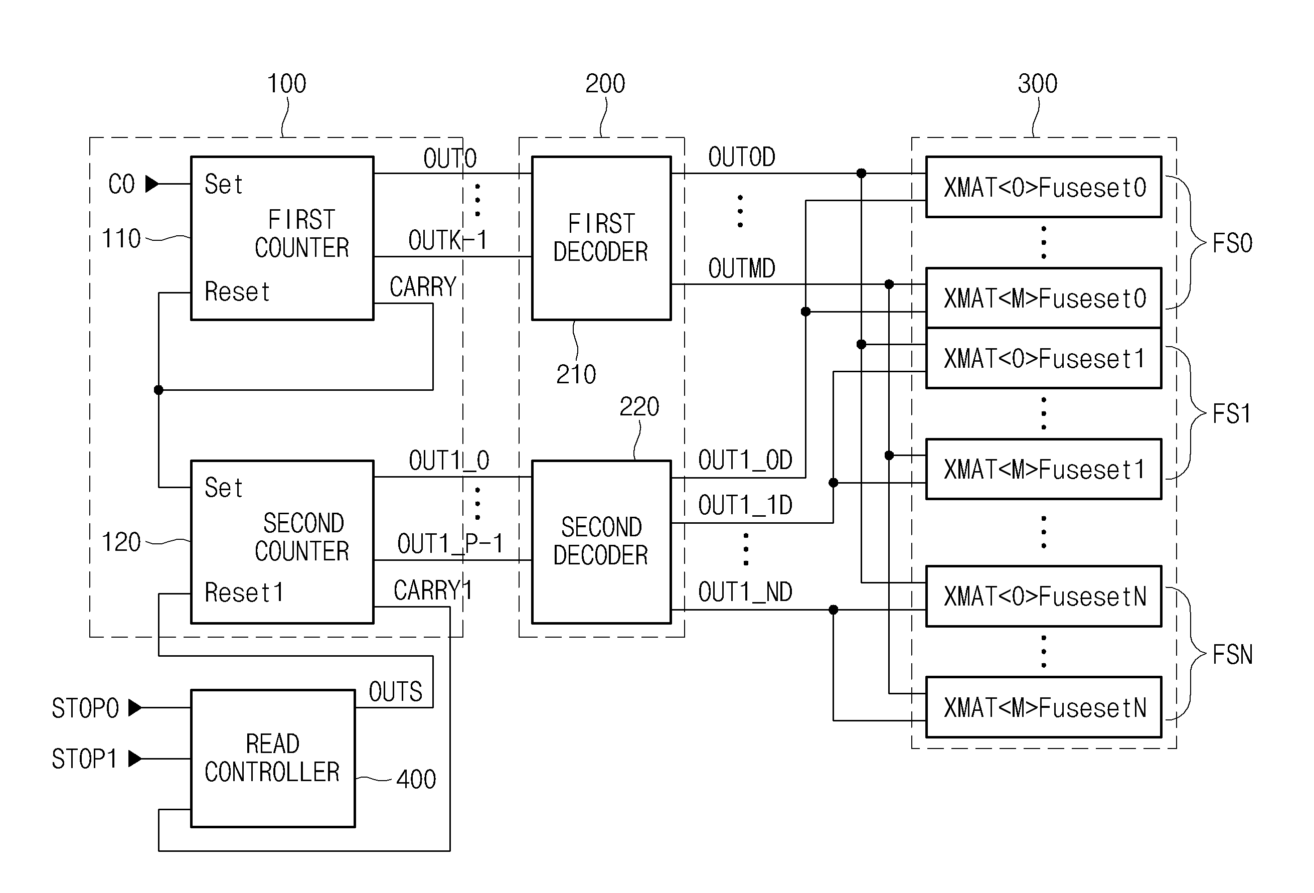
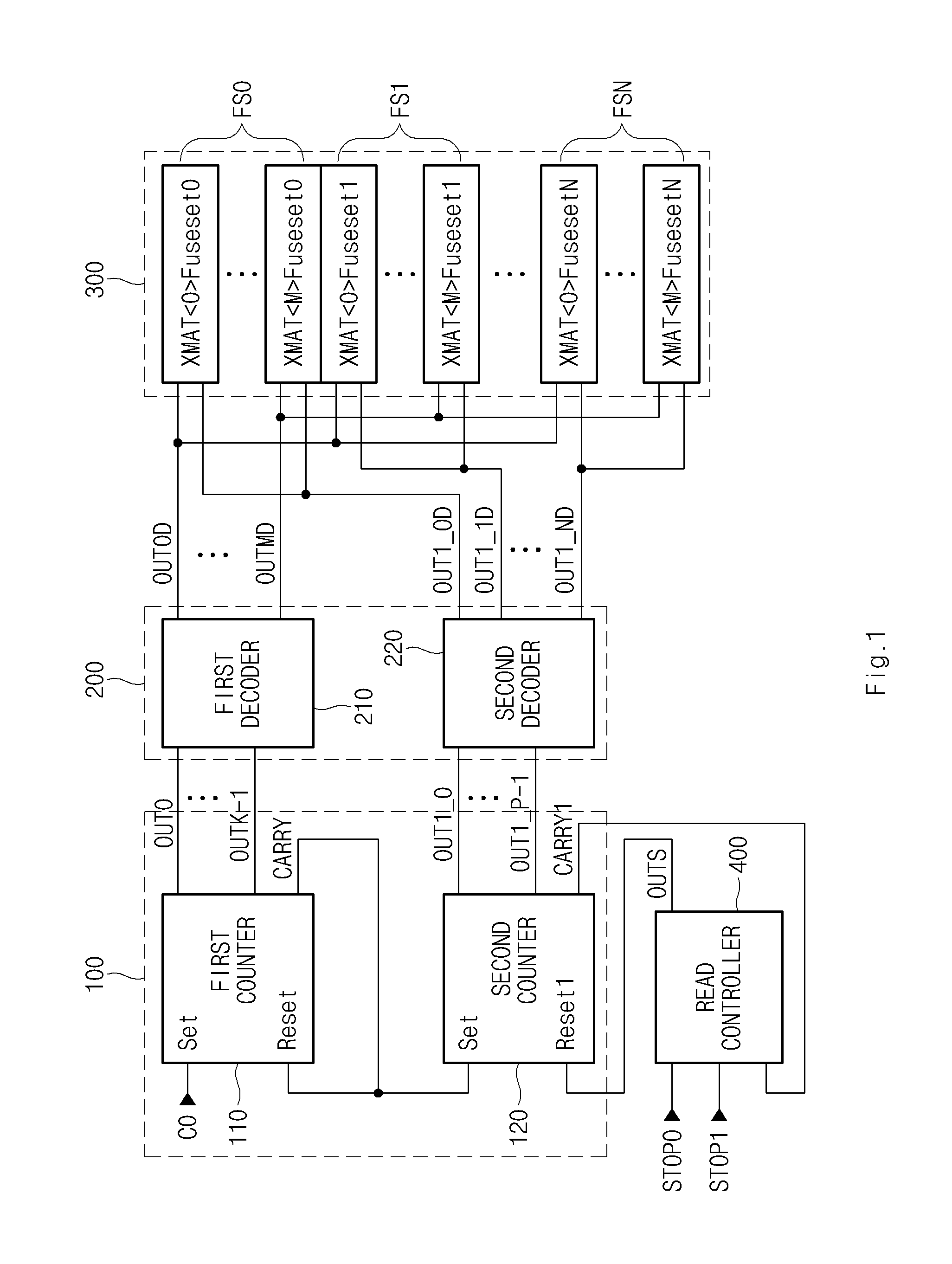
[0013]Embodiments of the present invention are described below in more detail with reference to the accompanying drawings. The present invention may, however, be embodied in different forms and should not be construed as limited to the embodiments set forth herein.

[0014]A redundancy control circuit may be used to solve the defective memory cell problem mentioned briefly above. If a defect occurs in any one of the memory cells, the redundancy control circuit recognizes the occurrence of the defect in the cell through testing. Thereafter, upon receiving an access request for the corresponding cell, the redundancy control circuit switches the connection to a cell contained in the redundancy circuit, instead of proceeding with the requested connection to the defective cell. The redundancy circuit is effectively an aggregate of redundant memory cells, and can be used as a substitute for a defective cell.

[0015]If a defect occurs in a normal memory cell, a redundancy memory cell is used to...


PUM


Abstract

A semiconductor device and method of operation having reduced read time of fuse array information during boot-up operation. When fuse array information is read, only repaired fuse-set information is read such that a read time of the semiconductor memory device is reduced, resulting in an increased read margin.

Description

CROSS-REFERENCE TO RELATED APPLICATION[0001]This application claims priority based upon Korean patent application No. 10-2012-0150998, filed on Dec. 21, 2012, the disclosure of which is hereby incorporated in its entirety by reference herein.BACKGROUND OF THE INVENTION[0002]The present invention relates generally to a semiconductor device and method of operation, and more particularly to a technology for reducing read time of a semiconductor device including a fuse array.[0003]A semiconductor memory device includes numerous memory cells. As fabrication technology has improved, the degree of integration of semiconductor memory devices has also increased, such that the number of memory cells has rapidly increased. If a defect occurs in one of the memory cells, there is a high probability that the corresponding semiconductor memory device will fail to perform properly. Generally, semiconductor memory devices in which defective memory cells are detected are simply discarded.[0004]Howeve...

Claims


Application Information

Patent Timeline
Patent Type & Authority Patents(United States)
IPC IPC(8): G11C17/00G11C17/16G11C8/10G11C29/00
CPCG11C17/16G11C8/10G11C29/787G11C17/165G11C5/148G11C7/20G11C17/18G11C29/785G11C2029/4402G11C7/10G11C29/00
Inventor LEE, JOO HYEONCHUN, JUN HYUNSONG, HO UK
Owner SK HYNIX INC
Why Eureka
Try Eureka