

Liquid crystal display device and driving method thereof
a liquid crystal display device and driving method technology, applied in the direction of electric digital data processing, instruments, computing, etc., can solve the problems of complicated logic circuits, logic controller control algorithms, and many line memories of impulsive driving methods, so as to minimize the capacitance of memory for storing data and simplify hardware construction.
- Summary
- Abstract
- Description
- Claims
- Application Information
AI Technical Summary
Benefits of technology
Problems solved by technology
Method used
Image

Examples
first exemplary embodiment
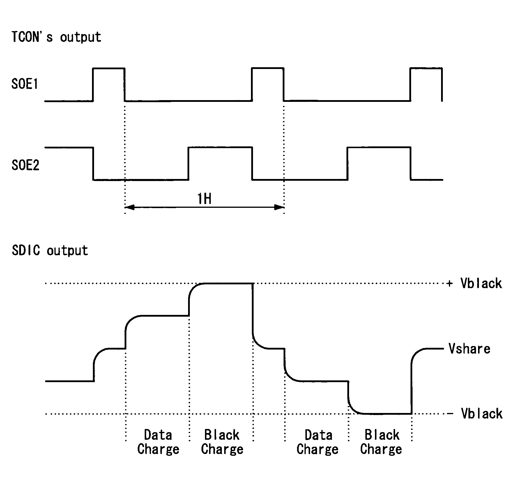
[0068]FIG. 10 is a diagram showing scanning operations of the video data voltages and black voltages according to a first exemplary embodiment, FIG. 11 is a waveform diagram showing the video data and black voltages charged in the liquid crystal cell by the scanning operation as shown in FIG. 10, and FIG. 12A is a timing diagram showing the gate timing control signals GSP1, GSC and GOE1 to GOE3, the first and the second source output enable signals SOE1 and SOE2, and the gate pulses G1 to G6 generated for period T1 of FIG. 10. In FIG. 12A, a letter ‘D’ indicated in the gate pulses G1 to G6 means the data voltages charged in the liquid crystal cells. FIG. 12B is a timing diagram showing the gate timing control signal GSP2, a first and a second source output enable signals SOE1 and SOE2, and the gate pulses G1 to G6 generated for period T3 of FIG. 10. In FIG. 12B, a letter ‘B’ indicated in the gate pulses G1 to G6 means the black voltage charged in the liquid crystal cells.
[0069]Refer...
second exemplary embodiment
[0081]FIG. 13 is a diagram showing scanning operations of video data voltages and black voltages according to a second exemplary embodiment of this invention, FIG. 14 is a waveform diagram showing voltages charged in a liquid crystal cell by the scanning operations of FIG. 13, and FIG. 15A is a timing diagram showing the gate timing control signals GSP1, GSC, and GOE1 to GOE3, the first and second source output enable signals SOE1 and SOE2, and the gate pulses G1 o to G6 generated for period T1 of FIG. 13. In FIG. 15a, a letter indicated in the gate pulses G1 to G6 means the black voltage charged in the liquid crystal cells. FIG. 15B is a timing diagram showing the gate timing control signals GSP2, GSC and GOE1 to GOE3, the first and second source output enable signals SOE1 and SOE2, and the gate pulses generated for period T3 of FIG. 13. In FIG. 15a, a letter ‘D’ indicated in the gate pulses G1 to G6 means the black voltage charged in the liquid crystal cells.
[0082]Referring to FIG...
PUM
 Abstract
Description
Claims
Application Information