Display device including a data selector circuit
a technology of selector circuit and display device, which is applied in the field of display device, can solve problems such as noise generation in the display panel, and achieve the effect of suppressing voltage variations and suppressing noise in the panel surfa
- Summary
- Abstract
- Description
- Claims
- Application Information
AI Technical Summary
Benefits of technology
Problems solved by technology
Method used
Image
Examples
first embodiment
[0050][First Embodiment]
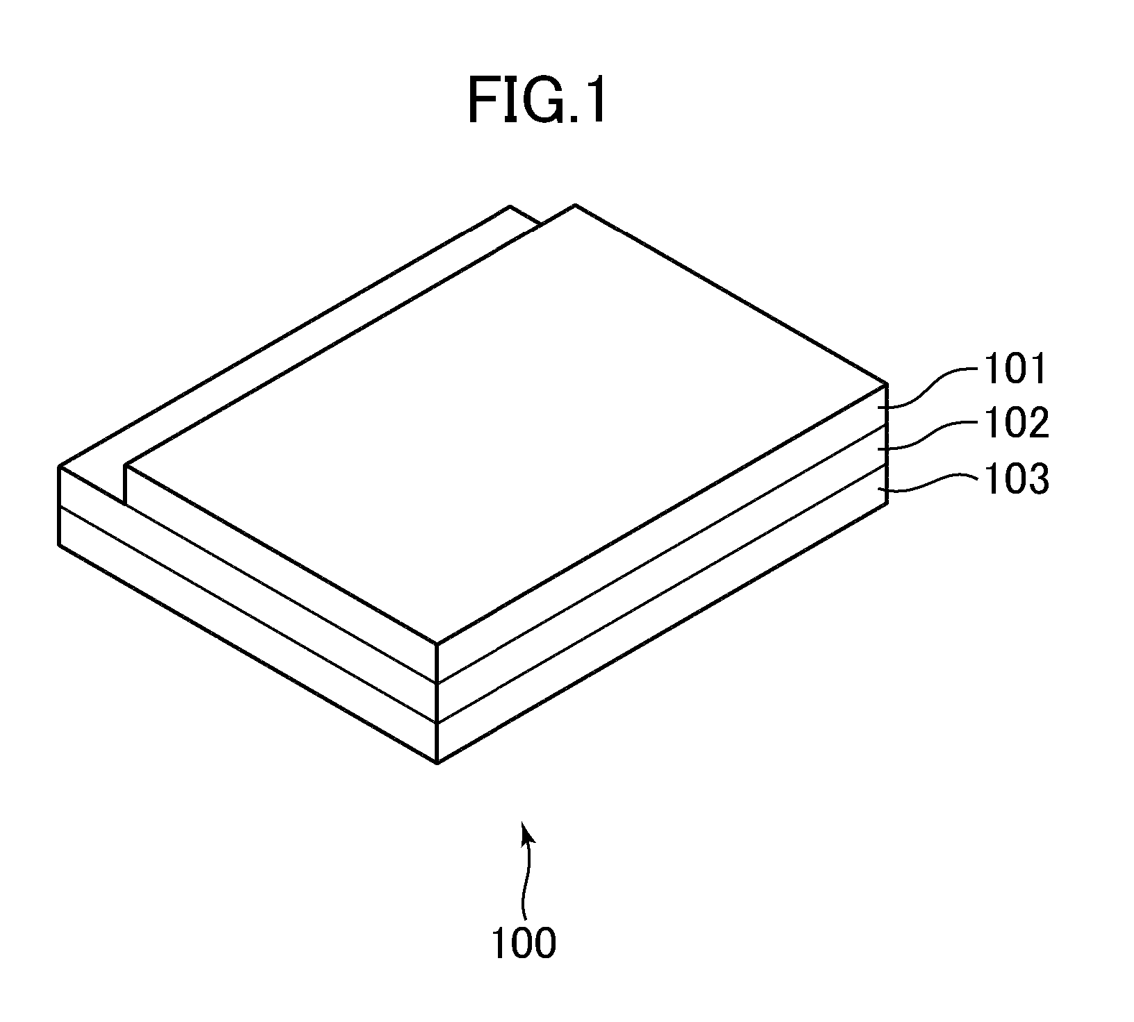
[0051]FIG. 1 is a diagram illustrating an outline of the display device according to the first embodiment of the present invention. As shown in FIG. 1, for example, a display device 100 includes a TFT substrate 102 provided with TFTs (not shown) and the like, and a filter substrate 101 which is opposite to the TFT substrate 102 and is provided with color filters (not shown). In addition, the display device 100 includes a liquid crystal material (not shown), which is sealed in a region interposed between the TFT substrate 102 and the filter substrate 101, and a backlight 103, which is located so as to come into contact with an opposite side of the filter substrate 101 side of the TFT substrate 102.
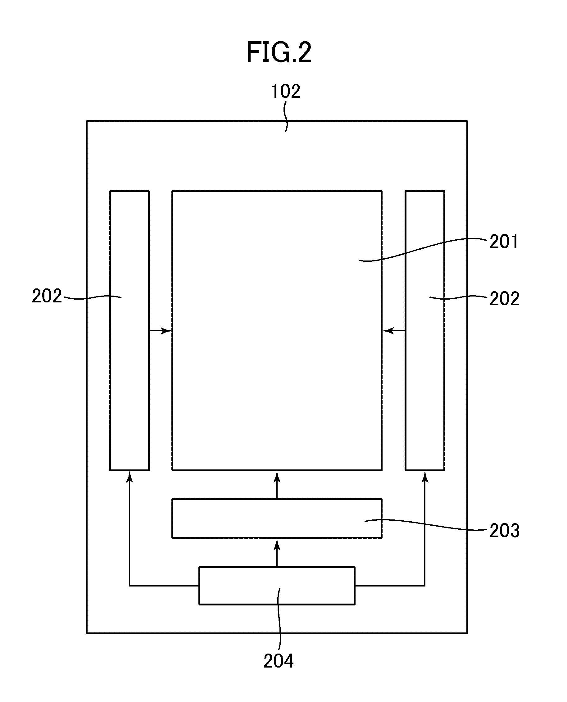
[0052]FIG. 2 is a diagram illustrating an outline of the configuration of the display device of one or more embodiments of the present invention. As shown in FIG. 2, the display device 100 includes a display region 201, gate circuits 202, a data selector circuit 203,...
second embodiment
[0086][Second Embodiment]
[0087]Next, a second embodiment of the present invention will be described. The second embodiment is mainly different from the first embodiment in that polarities are reversed for each data line when precharge and writing are performed in the data selector circuit 203. In addition, in the following, description of the same configuration as in the first embodiment will be omitted.
[0088]FIG. 8 is a diagram illustrating an example of the data selector circuit according to the second embodiment. As shown in FIG. 8, similarly to the first embodiment, the data selector circuit 203 includes input terminals 5a and 5b to which data signals are input from the driver 204, plural time division switches SW1 to SW6, and plural timing adjustment switches TSW1 to TSW6. Output sides of plural time division switches SW1 to SW6 and plural timing adjustment switches TSW1 to TSW6 are respectively connected to the data lines D1 to D6 (corresponding to the data lines 302). In addi...
third embodiment
[0094][Third Embodiment]
[0095]Next, a third embodiment of the present invention will be described. The third embodiment is mainly different from the first embodiment in that each of the input terminals 5a and 5b, to which a data signal is input from the driver 204, is divided into three, the data signal is input to corresponding time division switches SW1 to SW6, and polarities are reversed for each of the data lines D1 to D6 when precharge voltages and data signals are written, in a configuration of the data selector circuit 203. In addition, in the following, description of the same configuration as in the first embodiment will be omitted.
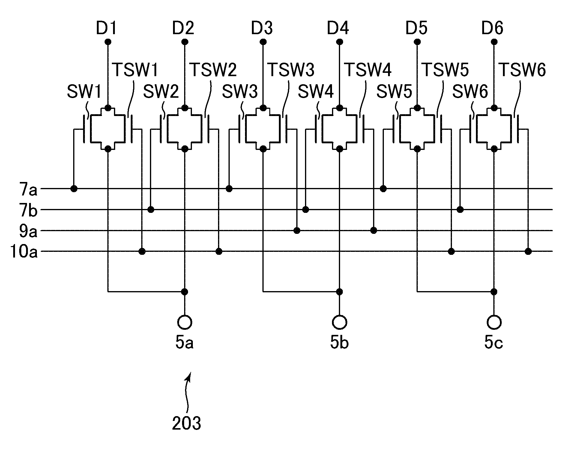
[0096]FIG. 9 is a diagram illustrating an example of the data selector circuit according to the third embodiment. In the present embodiment, similarly to the first embodiment, the data selector circuit 203 includes input terminals 5a and 5b to which data signals are input from the driver 204, plural time division switches SW1 to SW6, and plural t...
PUM
 Abstract
Description
Claims
Application Information


