Selective formation of metallic films on metallic surfaces

a technology of metallic surfaces and selective metal caps, applied in the direction of coatings, metallic material coating processes, chemical vapor deposition coatings, etc., can solve the problems of small devices, sharp decrease in the mean time to failure, and difficulty in implementing a selective metal cap

Active Publication Date: 2015-02-17
ASM INTERNATIONAL
View PDF11 Cites 410 Cited by
  • Summary
  • Abstract
  • Description
  • Claims
  • Application Information

AI Technical Summary

Problems solved by technology

Meeting the ever increasing electromigration (EM) requirement in copper interconnects is becoming more difficult as Moore's law progresses, resulting in smaller devices.
As line dimensions shrink, critical void size for EM failure is also reduced, causing a sharp decrease in mean time to failure.
The implementation of a selective metal cap has been challenging because of the difficulty in achieving good selectivity on copper versus the dielectric surface.

Method used


Image

  • Selective formation of metallic films on metallic surfaces
  • Selective formation of metallic films on metallic surfaces
  • Selective formation of metallic films on metallic surfaces

Examples


example 1

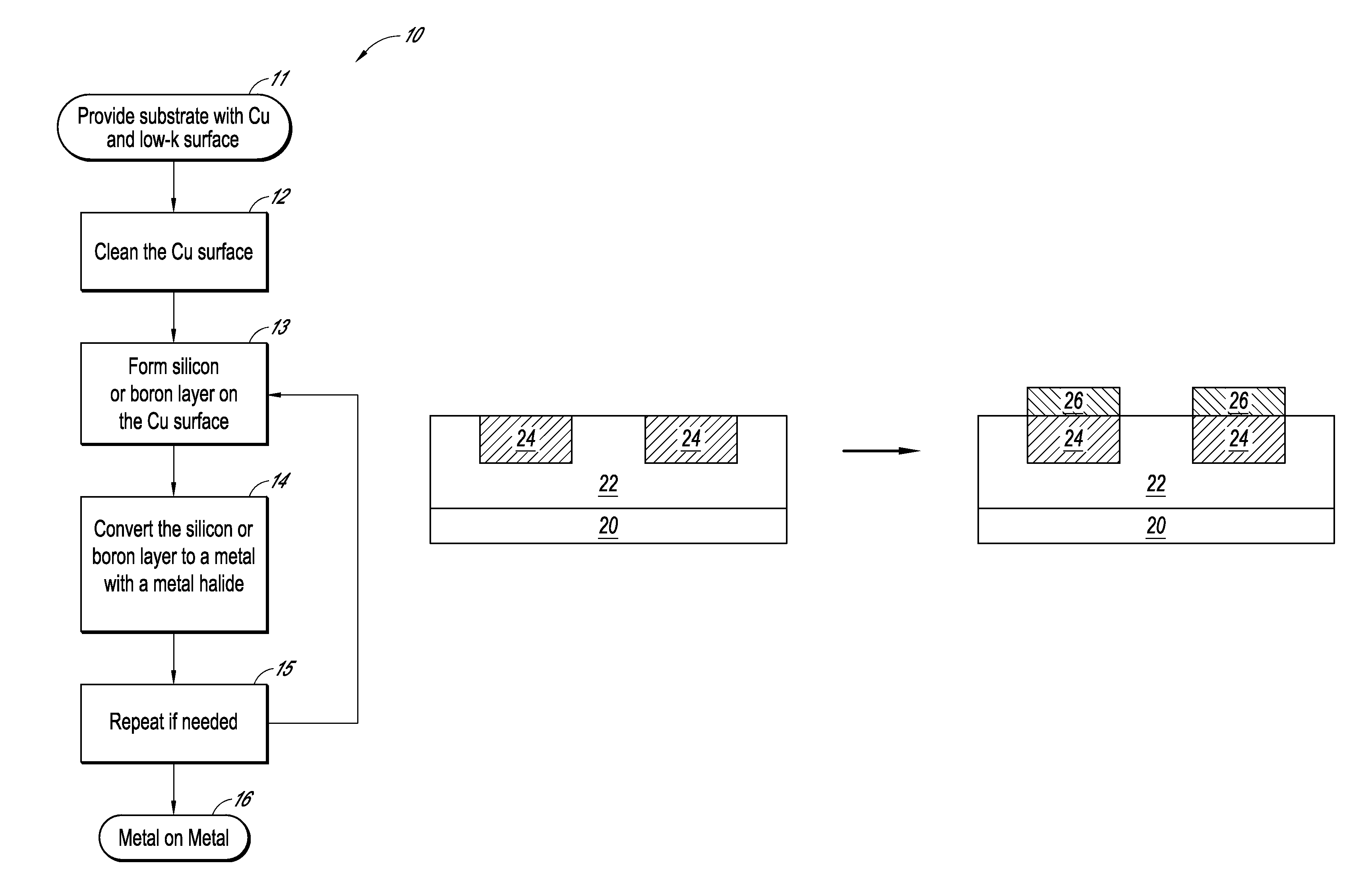
[0082]To selectively deposit a metallic layer on a metal surface, for example, the surface is preferably very clean. The cleaning may be conducted via gas or liquid phase. Specifically for copper, citric acid or some other later-generation cleaning agents may be used in the liquid phase to remove the commonly employed benzotriazole (BTA) passivating agent from the surface. Alternatively, NH3 plasma may be used as a gas phase approach to remove the BTA layer. Finally, H-radicals are used to ensure the surface is void of any oxidized copper.

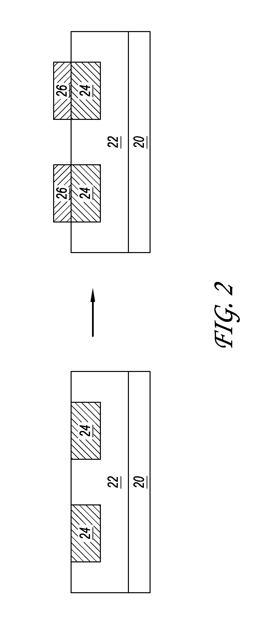
[0083]FIGS. 2 and 3 show schematic representations in accordance with some embodiments. FIG. 2 illustrates a substrate 20 with a silicon dioxide 22 insulating region and a copper surface 24. Selective deposition (not shown) is performed to deposit metal 26 on the copper regions 24 of the substrate while avoiding deposition on the SiO2 22.

[0084]FIG. 3 shows a schematic representation of a selective deposition process using disilane and WF6. The subs...

example 2

[0086]A copper piece was cut and cleaned with citric acid. The citric acid solution was prepared by mixing approximately 5 g of citric acid crystals in 50 ml of water. The solution was stirred until all crystals had dissolved. A fresh solution was prepared for each film deposition run and discarded immediately after use. The copper piece was dipped in the solution, left immersed for 30 seconds, and stirred a few times during that period. The copper piece was then lifted and dried by draining the liquid back into the solution. If the piece was dried by nitrogen blowing, water marks were produced. Finally, the back side of the copper piece was dried by placing the piece on a piece of clean room tissue. The cleaned copper piece was then placed onto an adapter wafer and loaded into a vacuum load lock within three minutes of cleaning.

[0087]After loading the copper piece into the vacuum load lock, it was transported by vacuum transport into the reaction chamber. The film deposition took p...


PUM

PropertyMeasurementUnit
temperatureaaaaaaaaaa
timeaaaaaaaaaa

Abstract

Metallic layers can be selectively deposited on surfaces of a substrate relative to a second surface of the substrate. In preferred embodiments, the metallic layers are selectively deposited on copper instead of insulating or dielectric materials. In preferred embodiments, a first precursor forms a layer or adsorbed species on the first surface and is subsequently reacted or converted to form a metallic layer. Preferably the deposition temperature is selected such that a selectivity of above about 90% is achieved.

Description

BACKGROUND OF THE INVENTION[0001]1. Field of the Invention[0002]The present application relates generally to the field of semiconductor fabrication.[0003]2. Description of the Related Art[0004]Integrated circuits are currently manufactured by an elaborate process in which various layers of materials are sequentially constructed in a predetermined arrangement on a semiconductor substrate.[0005]Meeting the ever increasing electromigration (EM) requirement in copper interconnects is becoming more difficult as Moore's law progresses, resulting in smaller devices. As line dimensions shrink, critical void size for EM failure is also reduced, causing a sharp decrease in mean time to failure. A significant improvement in EM resistance is required to enable continued scaling.[0006]The interface between the dielectric diffusion barrier and copper has been shown to be the main path for copper diffusion and the weakest link in resisting EM failure. The implementation of a selective metal cap ha...

Claims


Application Information

Patent Timeline
Patent Type & Authority Patents(United States)
IPC IPC(8): H01L21/44C23C16/02C23C16/14C23C16/455H01L21/02H01L21/285H01L21/768
CPCH01L21/02697C23C16/0227C23C16/14C23C16/45525H01L21/28562H01L21/76826H01L21/76829H01L21/76849H01L21/76883H01L21/0228H01L21/28194H01L21/76838H01L21/02068H01L21/32051H01L21/32053H01L21/7685
Inventor HAUKKA, SUVI P.NISKANEN, ANTTITUOMINEN, MARKO
Owner ASM INTERNATIONAL
Why Eureka
Try Eureka