Semiconductor device and manufacturing method thereof

a semiconductor device and manufacturing method technology, applied in the direction of coatings, transistors, chemical vapor deposition coatings, etc., can solve the problems of semiconductor device malfunction, increase in leakage current, increase in capacitor leakage current,

Active Publication Date: 2005-07-14
RENESAS ELECTRONICS CORP +1
View PDF6 Cites 128 Cited by
  • Summary
  • Abstract
  • Description
  • Claims
  • Application Information

AI Technical Summary

Benefits of technology

[0008] An object of the present invention is to provide a semiconductor device in which generation of an irregularly grown object in a TiN film is suppressed even when the deposition temperature of the TiN film is lowered to at most 450° C., and further to at most 400° C. in the CVD method, and a manufacturing method thereof.

Problems solved by technology

However, in a case of an MIS (Metal Insulator Silicon) capacitor in which polysilicon is used for the lower electrode and an MIM (Metal Insulator Metal) capacitor in which metal or a metal conductive nitride is used for the lower electrode, there has been a problem that leakage current in the capacitor increases if a TiN film of the upper electrode is formed at 600° C. Accordingly, the TiN film has been formed at the deposition temperature that is lowered to 400° C.-500° C.
This may result in malfunction of the semiconductor device.
Here, crystallization occurs by the thermal hysteresis of 450° C.-500° C. with the aforementioned metal oxide of high permittivity, and an electric conduction through grain boundary of crystals or defect level resulted thereby may undesirably increase the leakage current.

Method used


Image

  • Semiconductor device and manufacturing method thereof
  • Semiconductor device and manufacturing method thereof
  • Semiconductor device and manufacturing method thereof

Examples


first embodiment

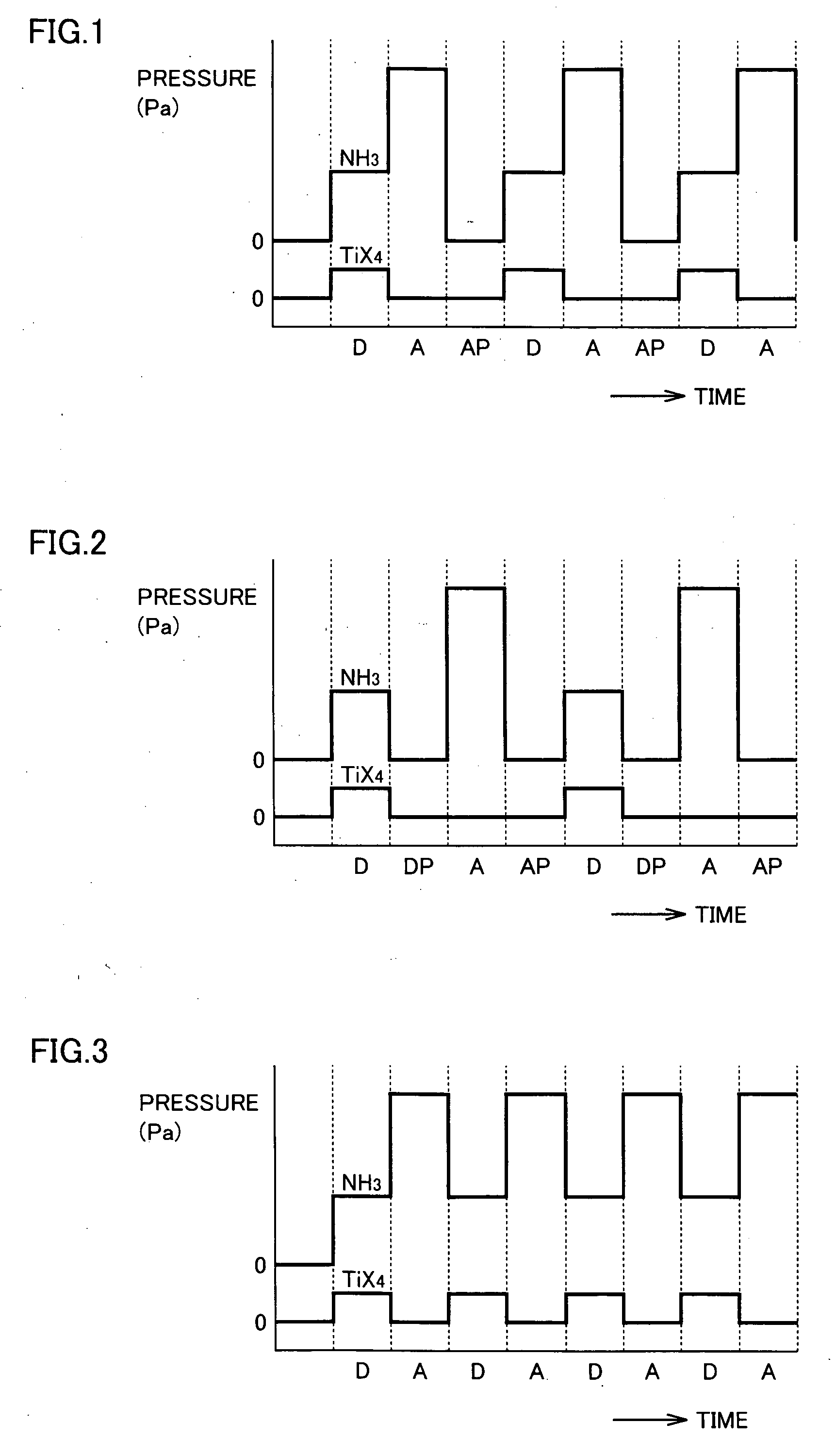
[0028] Referring to FIG. 1, a manufacturing method of a semiconductor device according to the present invention is a manufacturing method of a semiconductor device including a TiN film, including a deposition step (D step) of forming a TiN film by the CVD method, an anneal step (A step) of performing a heat treatment to the formed TiN film in an ammonium (NH3) gas atmosphere, an NH3 gas purge step (AP step) of purging NH3 gas, and a step of further repeating the deposition step, the anneal step, and the NH3 gas purge step for at least one time. The deposition step is performed using titanium halide gas and NH3 gas as material gases, and under a condition of a deposition temperature of 300° C.-450° C., a deposition pressure of 10 Pa-100 Pa, a partial pressure of titanium halide gas of 1 Pa-10 Pa, and a partial pressure of NH3 gas of 9 Pa-99 Pa. The TiN film is formed by a thickness of 1 nm-5 nm for each deposition step, and the anneal step is performed for 2 seconds to 60 seconds. Wi...

second embodiment

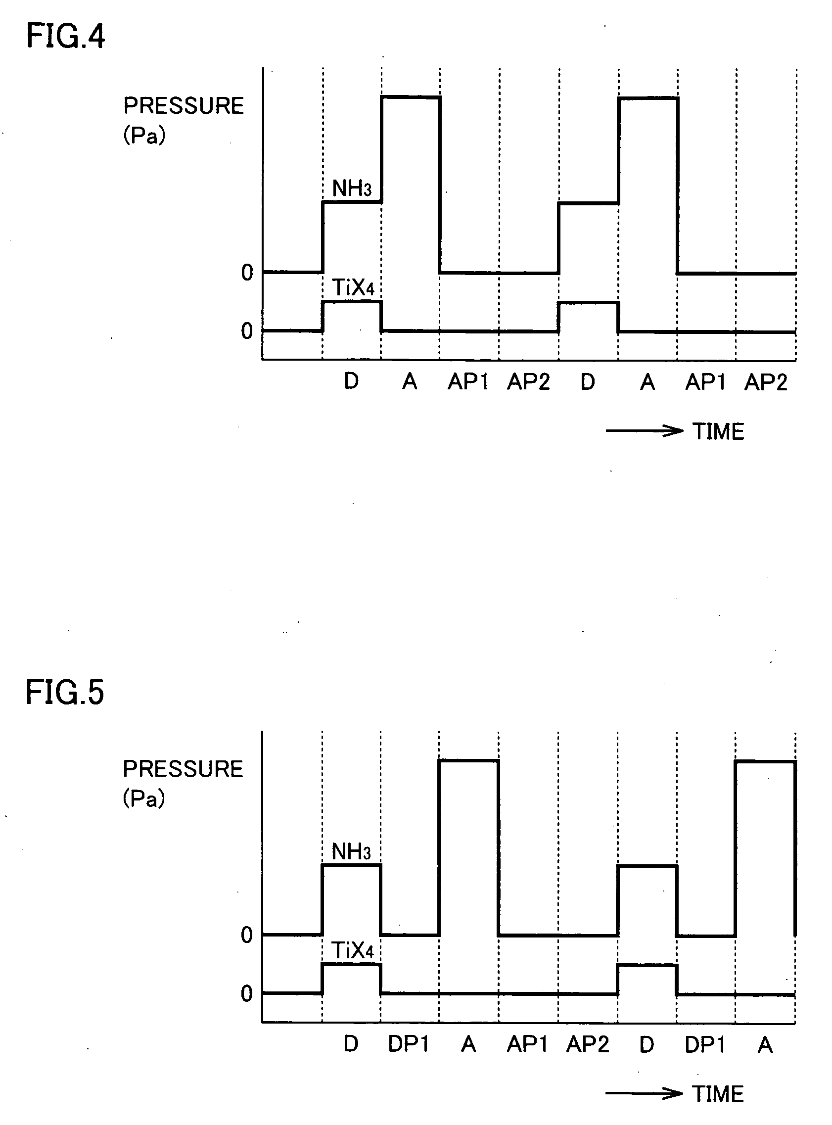
[0040] Referring to FIG. 2, another manufacturing method of a semiconductor device according to the present invention is a manufacturing method of a semiconductor device including a TiN film, including a deposition step (D step) of forming a TiN film by the CVD method, a material gas purge step (DP step) of purging a material gas, an anneal step (A step) of performing a heat treatment to the formed TiN film in an ammonium (NH3 ) gas atmosphere, an NH3 gas purge step (AP step) of purging NH3 gas, and a step of further repeating the deposition step, the material gas purge step, the anneal step, and the NH3 gas purge step for at least one time. The deposition step is performed using titanium halide gas and NH3 gas as material gases, and under a condition of a deposition temperature of 300° C. -450° C., a deposition pressure of 10 Pa-100 Pa, a partial pressure of titanium halide gas of 1 Pa-10 Pa, and a partial pressure of NH3 gas of 9 Pa-99 Pa. The TiN film is formed by a thickness of ...

third embodiment

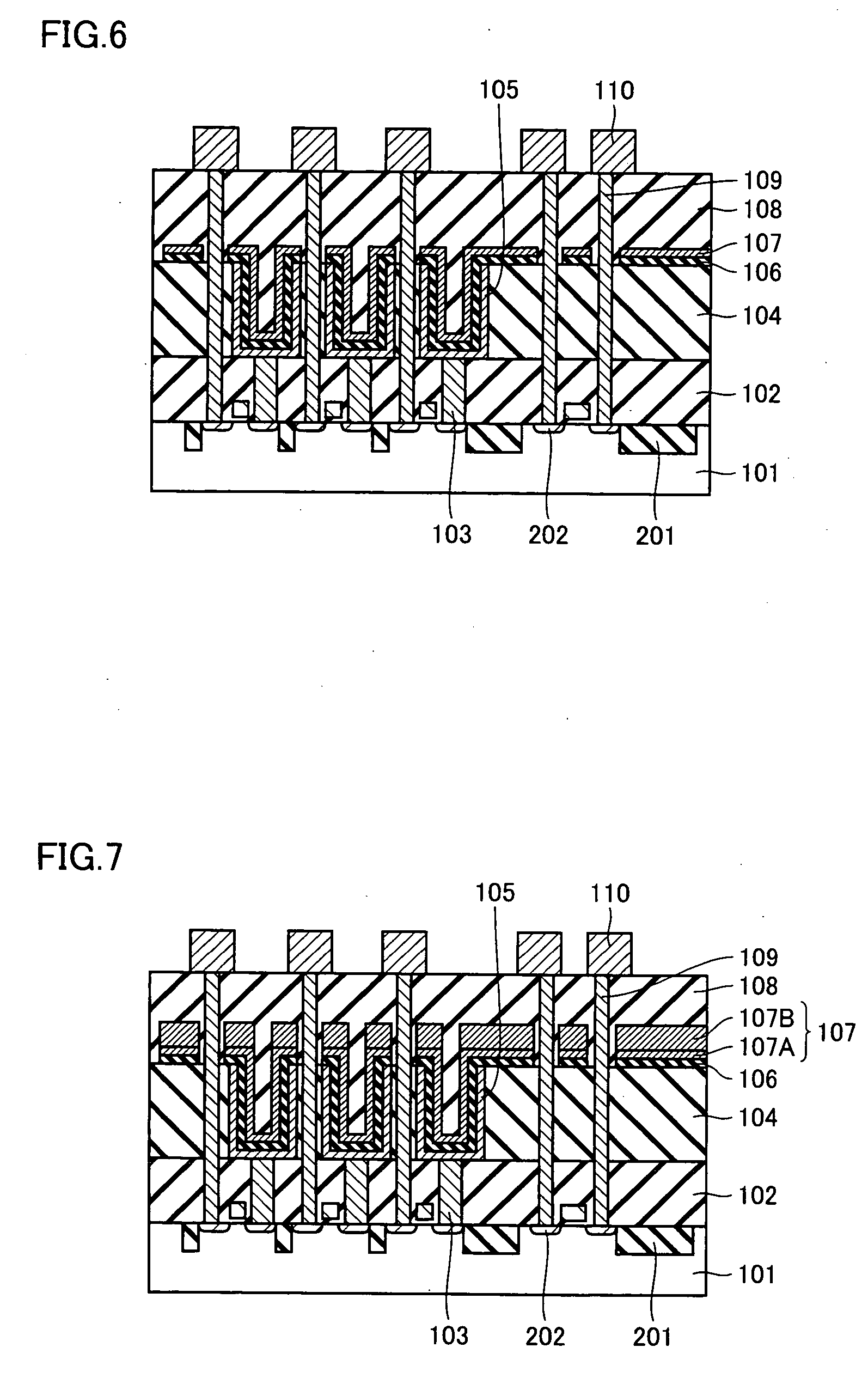
[0045] Referring to FIG. 3, another manufacturing method of a semiconductor device according to the present invention is a manufacturing method of a semiconductor device including a TiN film, including a deposition step (D step) of forming a TiN film by the CVD method, an anneal step (A step) of performing a heat treatment to the formed TiN film in an NH3 gas atmosphere, and a step of further repeating the deposition step and the anneal step for at least one time. The deposition step is performed using titanium halide gas and NH3 gas as material gases, and under a condition of a deposition temperature of 300° C.-450° C., a deposition pressure of 10 Pa-100 Pa, a partial pressure of titanium halide gas of 1 Pa-10 Pa, and a partial pressure of NH3 gas of 9 Pa-99 Pa. The TiN film is formed by a thickness of 1 nm-5 nm for each deposition step, and the anneal step is performed for 2 seconds to 60 seconds.

[0046] In the present embodiment, similarly to the first embodiment, though an annea...


PUM

PropertyMeasurementUnit
deposition temperatureaaaaaaaaaa
thicknessaaaaaaaaaa

Abstract

A manufacturing method of a semiconductor device including a TiN film, including a deposition step of forming a TiN film by the CVD method, an anneal step of performing a heat treatment to the formed TiN film in an atmosphere of NH3 gas, an NH3 gas purge step of purging NH3 gas, and a step of further repeating the deposition step, the anneal step, and the NH3 gas purge step for at least one time. The deposition step is performed using titanium halide gas and NH3 gas as material gases and with a deposition temperature of 300° C.-450° C. to form the TiN film by a thickness of 1 nm-5 nm for each deposition step. Thus, a semiconductor device in which generation of irregularly grown objects in the TiN film is suppressed and a manufacturing method thereof can be provided.

Description

BACKGROUND OF THE INVENTION [0001] 1. Field of the Invention [0002] The present invention relates to a semiconductor device having a titanium nitride film and a manufacturing method thereof. [0003] 2. Description of the Background Art [0004] Conventionally, in a capacitor in which a high dielectrics of a metal oxide such as Ta2O5, HfO2, BaSrTiO3 or the like is used as a dielectric layer, a titanium nitride film (hereinafter referred to as a TiN film) formed by the chemical vapor deposition method (hereinafter referred to as the CVD method) has been used as an upper electrode. Generally, the manufacturing condition of this TiN film involves use of titanium halide gas (for example, TiCl4 gas) and ammonium gas (NH3 gas) as material gases at a deposition temperature of about 600° C. [0005] However, in a case of an MIS (Metal Insulator Silicon) capacitor in which polysilicon is used for the lower electrode and an MIM (Metal Insulator Metal) capacitor in which metal or a metal conductive ...

Claims


Application Information

Patent Timeline
Patent Type & Authority Applications(United States)
IPC IPC(8): C23C16/34C23C16/44H01L21/20C23C16/56H01L21/02H01L21/28H01L21/285H01L21/336H01L21/8242H01L27/108H01L29/423H01L29/49H01L29/78
CPCC23C16/34C23C16/4408C23C16/56H01L28/60H01L21/28556H01L27/10811H01L27/10894H01L21/28088H10B12/312H10B12/09H01L21/20H01L21/18H10B99/00
Inventor OKUDAIRA, TOMONORIHAYASHI, TAKESHIFUJIWARA, HIROSHIFUJITA, YASUSHIKOBAYASHI, KIYOTERU
Owner RENESAS ELECTRONICS CORP
Why Eureka
Try Eureka