Low-temperature selective epitaxial growth of silicon for device integration

a technology of epitaxial growth and silicon, applied in the field of low-temperature epitaxial growth process, can solve the problems of low silicon epitaxial growth rate, limited process and application, and high temperature requirement limit the use of silicon epitaxial growth,

Inactive Publication Date: 2015-09-03
INT BUSINESS MASCH CORP
View PDF8 Cites 173 Cited by
  • Summary
  • Abstract
  • Description
  • Claims
  • Application Information

AI Technical Summary

Problems solved by technology

However, conventional methods for SEG of silicon require high temperature processing.
The high temperature requirement limits the processes and applications which can utilize the conventional methods for SEG of Si.
Further, conventional high temperature depositions (over 600 degrees C.) for epitaxial growth of silicon lack selective growth of Si on predetermined areas, e.g., where the c-Si is exposed.

Method used


Image

  • Low-temperature selective epitaxial growth of silicon for device integration
  • Low-temperature selective epitaxial growth of silicon for device integration
  • Low-temperature selective epitaxial growth of silicon for device integration

Examples


Embodiment Construction

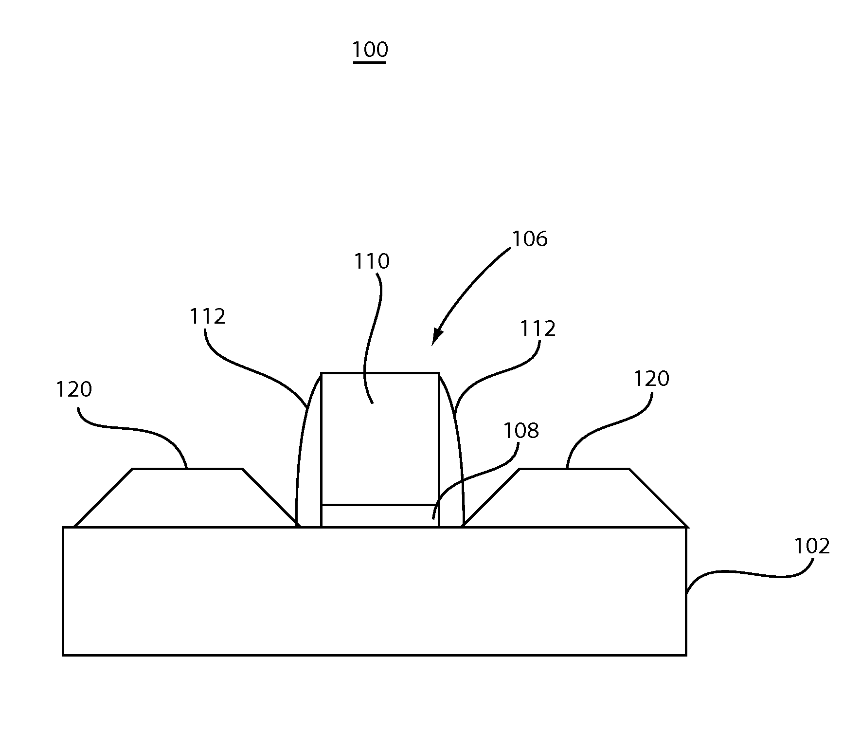
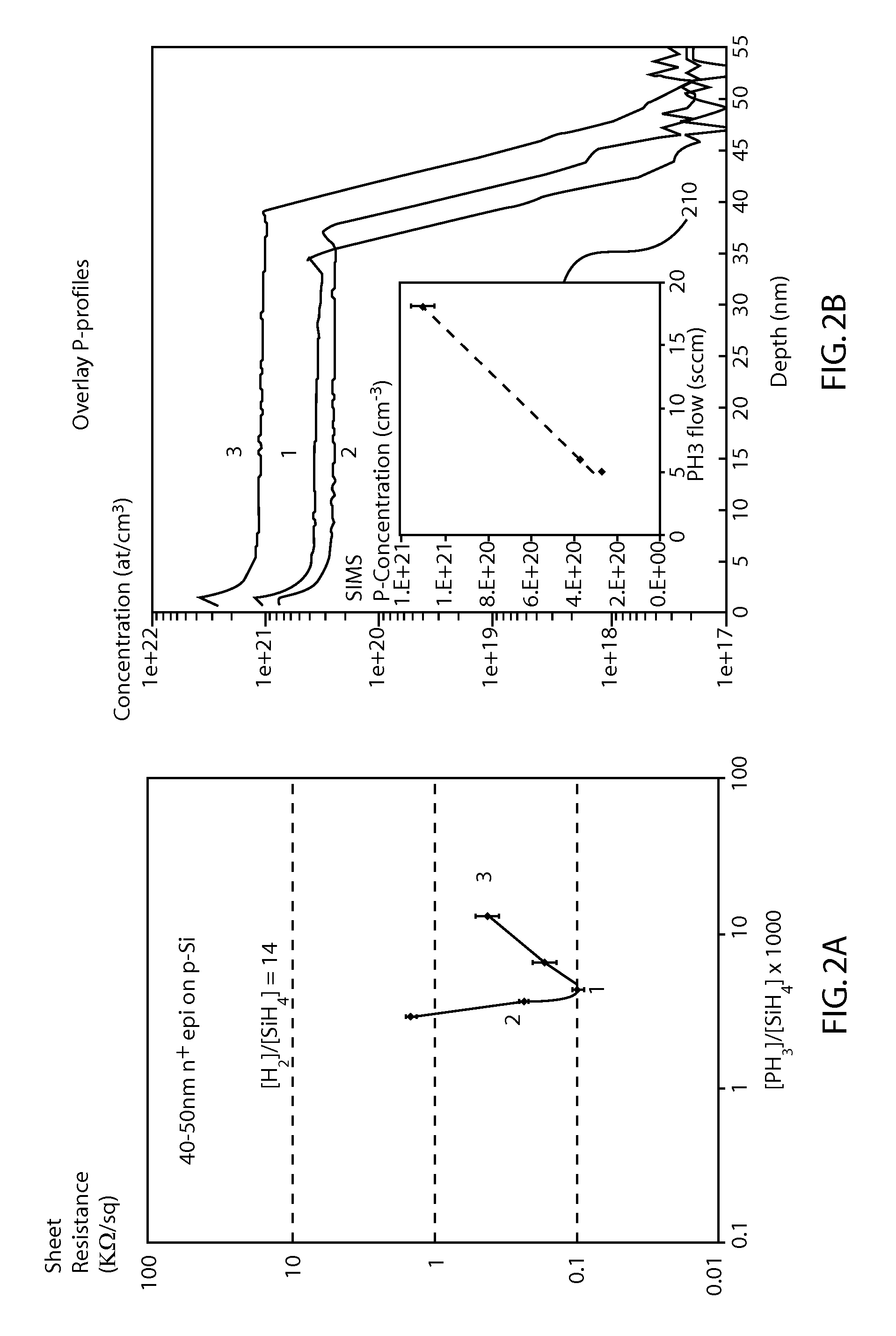
[0020]In accordance with the present principles, methods for selective epitaxial growth of highly-doped silicon at low temperatures are disclosed. In particularly useful embodiments, growth temperatures as low as 150° C. are achieved using plasma enhanced chemical vapor deposition (PECVD). The epitaxial growth is obtained by increasing and optimizing a gas ratio of [H2] / [SiH4]. In another embodiment, an N+ doped silicon is grown by, e.g., incorporating phosphorus using PH3 gas.

[0021]High dopant activation, e.g., greater than 1×1020 cm −3, can be obtained at 150° C. Selective growth is provided by etching a deposited silicon on regions where crystalline-Si (c-Si) is not exposed, in H2 plasma. As a result, the present embodiments offer an uninterrupted selective epitaxial growth (SEG) of Si, where the epitaxial growth and the plasma etching of the non-epitaxial Si occur in a same reactor. Selective epitaxial growth of boron doped Si or other dopants is also possible using the present ...


PUM

PropertyMeasurementUnit
temperatureaaaaaaaaaa
deposition temperatureaaaaaaaaaa
temperaturesaaaaaaaaaa

Abstract

An epitaxy method includes providing an exposed crystalline region of a substrate material. Silicon is epitaxially deposited on the substrate material in a low temperature process wherein a deposition temperature is less than 500 degrees Celsius. A source gas is diluted with a dilution gas with a gas ratio of dilution gas to source gas of less than 1000.

Description

RELATED APPLICATION DATA[0001]This application is a divisional application of U.S. patent application Ser. No. 13 / 032,866 filed on Feb. 23, 2011, incorporated herein by reference in its entirety.BACKGROUND[0002]1. Technical Field[0003]The present invention relates to semiconductor processing and more particularly to a low temperature epitaxial growth process.[0004]2. Description of the Related Art[0005]Selective epitaxial growth (SEG) of highly doped silicon is suitable for applications in raised source / drain (S / D) regions to reduce parasitic series resistance associated with shallow-doped S / D regions. However, conventional methods for SEG of silicon require high temperature processing. The typical processing temperatures are greater than 600° C.[0006]The high temperature requirement limits the processes and applications which can utilize the conventional methods for SEG of Si. Further, conventional high temperature depositions (over 600 degrees C.) for epitaxial growth of silicon l...

Claims


Application Information

Patent Timeline
Patent Type & Authority Applications(United States)
IPC IPC(8): C30B25/18C30B29/06C30B25/10
CPCC30B25/183C30B25/105C30B25/186C30B29/06C30B25/14H01L21/02576H01L21/02381H01L21/02395H01L21/02532H01L21/0262H01L21/02639C30B25/04C30B33/12H01L21/02584H01L21/3065
Inventor HEKMATSHOAR-TABARI, BAHMANKHAKIFIROOZ, ALIREZNICEK, ALEXANDERSADANA, DEVENDRA K.SHAHIDI, GHAVAM G.SHAHRJERDI, DAVOOD
Owner INT BUSINESS MASCH CORP
Why Eureka
Try Eureka