

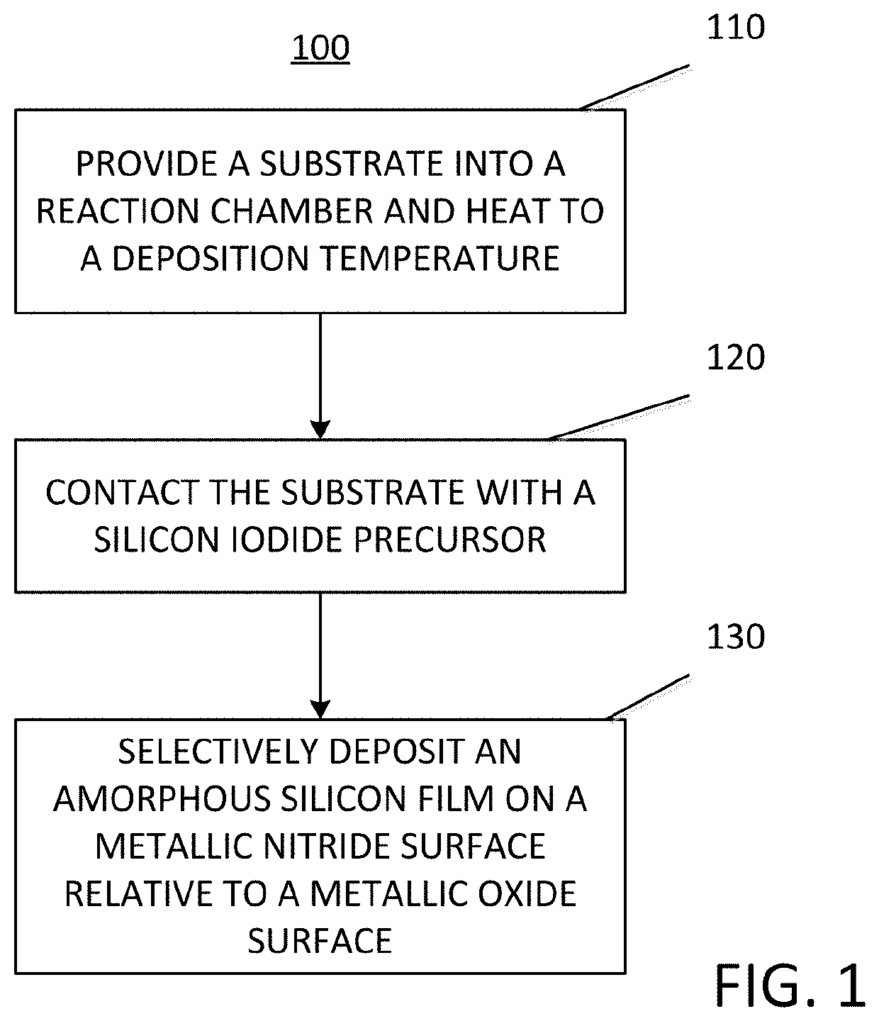
Methods for selectively depositing an amorphous silicon film on a substrate
a technology of amorphous silicon and amorphous film, which is applied in the direction of coating, chemical vapor deposition coating, metallic material coating process, etc., can solve the problems of low precision required for many applications, time-consuming and expensive lithography and etch process, and inability to meet the requirements of many applications
- Summary
- Abstract
- Description
- Claims
- Application Information
AI Technical Summary
Benefits of technology
Problems solved by technology
Method used
Image

Examples
Embodiment Construction
[0019]Although certain embodiments and examples are disclosed below, it will be understood by those in the art that the invention extends beyond the specifically disclosed embodiments and / or uses of the invention and obvious modifications and equivalents thereof. Thus, it is intended that the scope of the invention disclosed should not be limited by the particular disclosed embodiments described below.
[0020]As used herein, the term “substrate” may refer to any underlying material or materials that may be used, or upon which, a device, a circuit, or a film may be formed.
[0021]As used herein, the term “chemical vapor deposition” may refer to any process wherein a substrate is exposed to one or more volatile precursors, which react and / or decompose on a substrate surface to produce a desired deposition.
[0022]As used herein, the term “amorphous silicon film” may refer to a silicon film that exhibits substantially no long range ordering of the crystalline structure that would normally be...
PUM
| Property | Measurement | Unit |
|---|---|---|
| Temperature | aaaaa | aaaaa |
| Fraction | aaaaa | aaaaa |
| Pressure | aaaaa | aaaaa |
Abstract
Description
Claims
Application Information