
Electronic device including shallow trench isolation (STI) regions with bottom nitride liner and upper oxide liner and related methods

a technology of electrodes and electrodes, applied in the field of electromechanical devices, can solve problems such as shortening the time from the device source/drain region to the si substra

Active Publication Date: 2015-04-07
STMICROELECTRONICS SRL
View PDF9 Cites 7 Cited by
  • Summary
  • Abstract
  • Description
  • Claims
  • Application Information

AI Technical Summary

Benefits of technology

This patent describes an electronic device that has a structure called an STI region. This structure helps to prevent electrical shorts between certain parts of the device. This makes the device more reliable and efficient.

Problems solved by technology

However, with the ultra-thin layers, typical processing operations may cause divots at the interface of the STI regions that can result in shorting from the device source / drain regions to the Si substrate.

Method used


Image

  • Electronic device including shallow trench isolation (STI) regions with bottom nitride liner and upper oxide liner and related methods
  • Electronic device including shallow trench isolation (STI) regions with bottom nitride liner and upper oxide liner and related methods
  • Electronic device including shallow trench isolation (STI) regions with bottom nitride liner and upper oxide liner and related methods

Examples


Embodiment Construction

[0016]The present invention will now be described more fully hereinafter with reference to the accompanying drawings, in which preferred embodiments of the invention are shown. This invention may, however, be embodied in many different forms and should not be construed as limited to the embodiments set forth herein. Rather, these embodiments are provided so that this disclosure will be thorough and complete, and will fully convey the scope of the invention to those skilled in the art. Like numbers refer to like elements throughout.

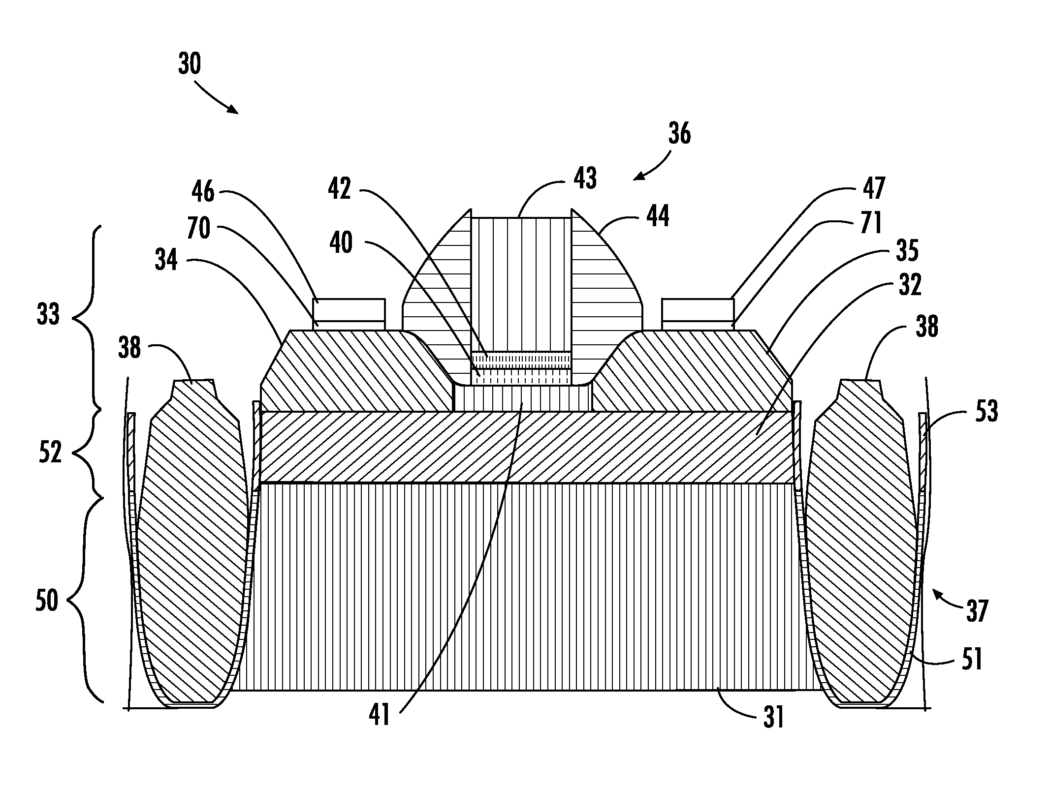
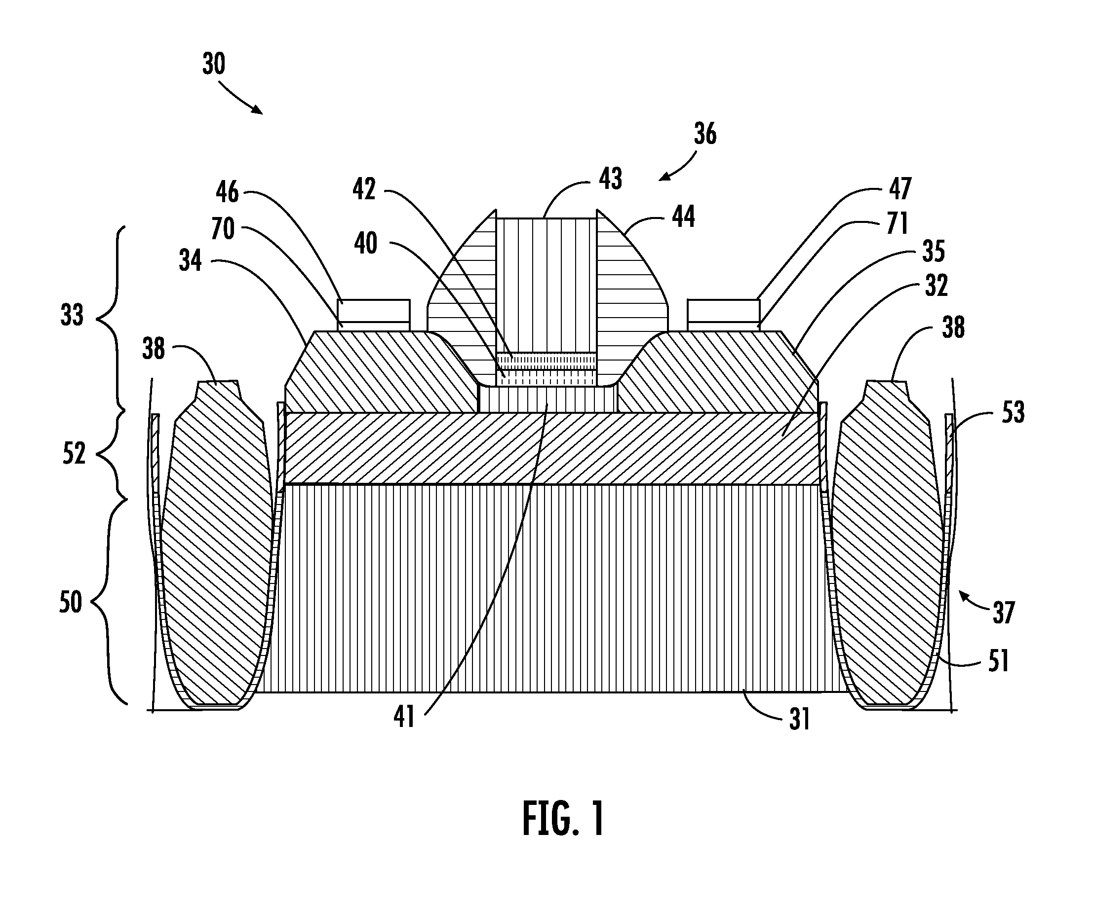
[0017]Referring initially to FIG. 1, an electronic device 30 is are first described. In the illustrated example, the electronic device 30 is a UTBB structure which illustratively includes a substrate 31, a buried oxide layer 32 overlying the substrate, and one or more semiconductor devices 33 overlying the BOX layer. In the illustrated example, the substrate 31 is a silicon substrate, although other suitable substrates (e.g., germanium, etc.) may also be u...


PUM


Abstract

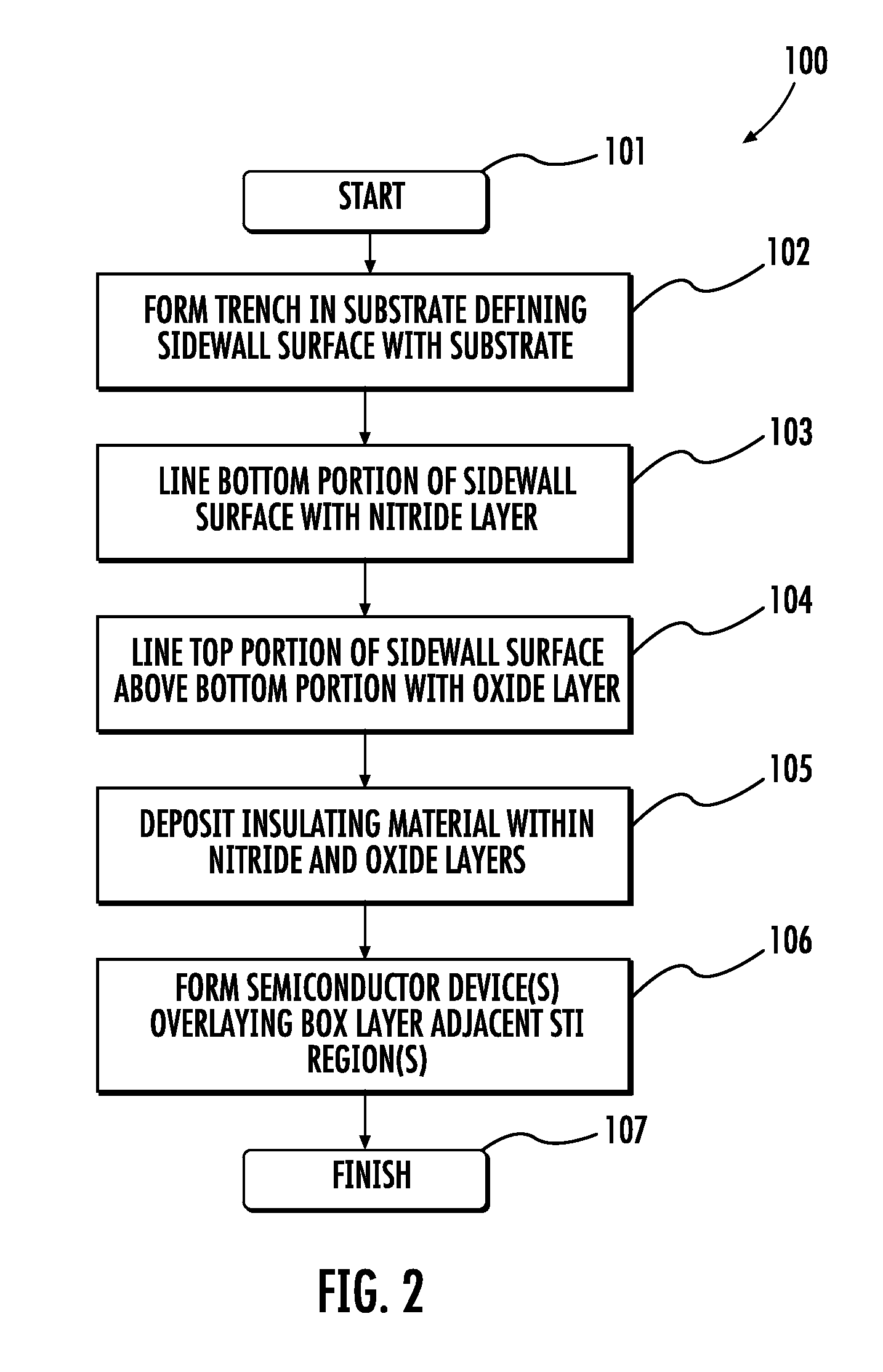
An electronic device may include a substrate, a buried oxide (BOX) layer overlying the substrate, at least one semiconductor device overlying the BOX layer, and at least one STI region in the substrate and adjacent the at least one semiconductor device. The at least one STI region defines a sidewall surface with the substrate and may include a nitride layer lining a bottom portion of the sidewall surface, an oxide layer lining a top portion of the sidewall surface above the bottom portion, and an insulating material within the nitride and oxide layers.

Description

FIELD OF THE INVENTION[0001]The present invention relates to the field of electronic devices and, more particularly, to semiconductor devices and related methods.JOINT RESEARCH AGREEMENT[0002]The claimed configurations set forth herein were made as a result of activities undertaken within the scope of a joint research agreement. The parties to the joint research agreement are (1) STMicroelectronics, Inc., and (2) International Business Machines Corporation.BACKGROUND OF THE INVENTION[0003]Ultra-thin Body and Buried Oxide (BOX) devices (UTBB) are an attractive device structure in that they may allow for improved semiconductor device scaling. UTBB typically includes an ultra-thin Si body as a channel region, which is fully depleted and is beneficial for short channel effect (SCE) control. Also, with thinner BOX (about 25 nm or thinner), compared with ETSOI (extreme thin silicon-on-insulator) devices which have a thicker BOX (more than 50 nm), UTBB provides better scaling capability an...

Claims


Application Information

Patent Timeline
Patent Type & Authority Patents(United States)
IPC IPC(8): H01L21/70H01L21/762
CPCH01L21/76283H01L21/76202H01L21/762H01L21/76264H01L21/76224
Inventor LIU, QINGLOUBET, NICOLASKHARE, PRASANNA
Owner STMICROELECTRONICS SRL
Learn More