
Architectural floorplan for a structured ASIC manufactured on a 28 NM CMOS process lithographic node or smaller

a technology of lithographic nodes and architectural floor plans, which is applied in the direction of logic circuit coupling/interface arrangements, pulse techniques, instruments, etc., can solve the problems of wasting significant power in transitions within blocks, wasting time and effort, and limiting the maximum performance of the entire system

Active Publication Date: 2015-05-05
INTEL CORP
View PDF35 Cites 3 Cited by
  • Summary
  • Abstract
  • Description
  • Claims
  • Application Information

AI Technical Summary

Benefits of technology

[0052]The sum total of all of the above advantages, as well as the numerous other advantages disclosed and inherent from the invention described herein, creates an improvement over prior techniques.

Problems solved by technology

While the layout of each cell in a standard cell is predetermined, the circuit itself has to be uniquely constructed by connecting all layers to one another and the cells within each layer in a custom manner, which takes time and effort.
The control of any differences and uncertainty in the arrival times of the clock signals can limit the maximum performance of the entire system and create race conditions in which an incorrect data signal may latch within a register.
The clock distribution network often takes a significant portion of the power consumed by a chip; furthermore, significant power can be wasted in transitions within blocks, when their output is not needed.
A simple PLD, historically called a programmable logic device, is much more limited in application, as they do not have a general interconnect structure.
These components are no longer supported by modern EDA (Electronic Design Automation) software and have very limited functionality.
However, optimizing multilevel synthesis logic is more difficult than optimizing two-level synthesis logic, and often employs heuristic techniques.
Design constraints in floorplanning include minimizing the silicon chip area and minimizing timing delay.
The determination of the MRST is in general a NP-complete problem—which is difficult to solve in a reasonable time.
For small numbers of terminals heuristic algorithms exist, but they are expensive in engineering cost to compute.
If a via is disabled, then it cannot practically conduct a signal, i.e., the via has very high resistance or does not physically exist.
If the clock signal arrives at different components at different times, there is clock skew.
Clock skew can be caused by many different things, such as wire-interconnect length, temperature variations and differences in input capacitance on the clock inputs of devices using the clock.
These are also the disadvantages of standard cell ASICs: they can be difficult to design, have longer development times, and higher NRE costs.
The disadvantages of FPGAs are that design size is limited to relatively small production designs, design complexity is limited, performance is limited, power consumption is high, and there is a high cost per unit.
These FPGA disadvantages are standard-cell advantages, as standard cells support large and complex designs, have high performance, low power consumption and low per-unit cost at a high volume.
The disadvantage of structured ASICs compared to FPGAs is that FPGAs do not require any user design information during manufacturing.
Fewer metal layers are needed for fabrication of a Structured ASIC, which dramatically reduces the turnaround time.
The unit cost of a Structured ASIC may be somewhat higher than a full custom ASIC, primarily due to the imperfect fit between design requirements and a standardized base layer, with certain I / O, memory and logic capacities.
The three modes of operation in a nMOS are called the cut-off, triode and saturation. nMOS logic is easy to design and manufacture, but devices made of nMOS logic gates dissipate static power when the circuit is idling, since DC current flows through the logic gate when the output is low.
Since CMOS circuits contain pMOS devices, which are affected by the lower hole mobility, CMOS circuits are not faster than their all-nMOS counter parts.

Method used


Image

  • Architectural floorplan for a structured ASIC manufactured on a 28 NM CMOS process lithographic node or smaller
  • Architectural floorplan for a structured ASIC manufactured on a 28 NM CMOS process lithographic node or smaller
  • Architectural floorplan for a structured ASIC manufactured on a 28 NM CMOS process lithographic node or smaller

Examples


Embodiment Construction

[0070]The method and apparatus of the present invention may be described in software, such as the representation of the invention in an EDA tool, or realized in hardwire, such as the actual physical instantiation.

[0071]Regarding the floorplan of the present invention, the drawings sometimes show elements as blocks that in a physical implementation may differ from this stylized representation, but the essential features of the floorplan should be apparent to one of ordinary skill in the art from the teachings herein.

[0072]The elements in the floor plan of the present invention are operatively connected to one another where necessary, as can be appreciated by one of ordinary skill in the art from the teachings herein.

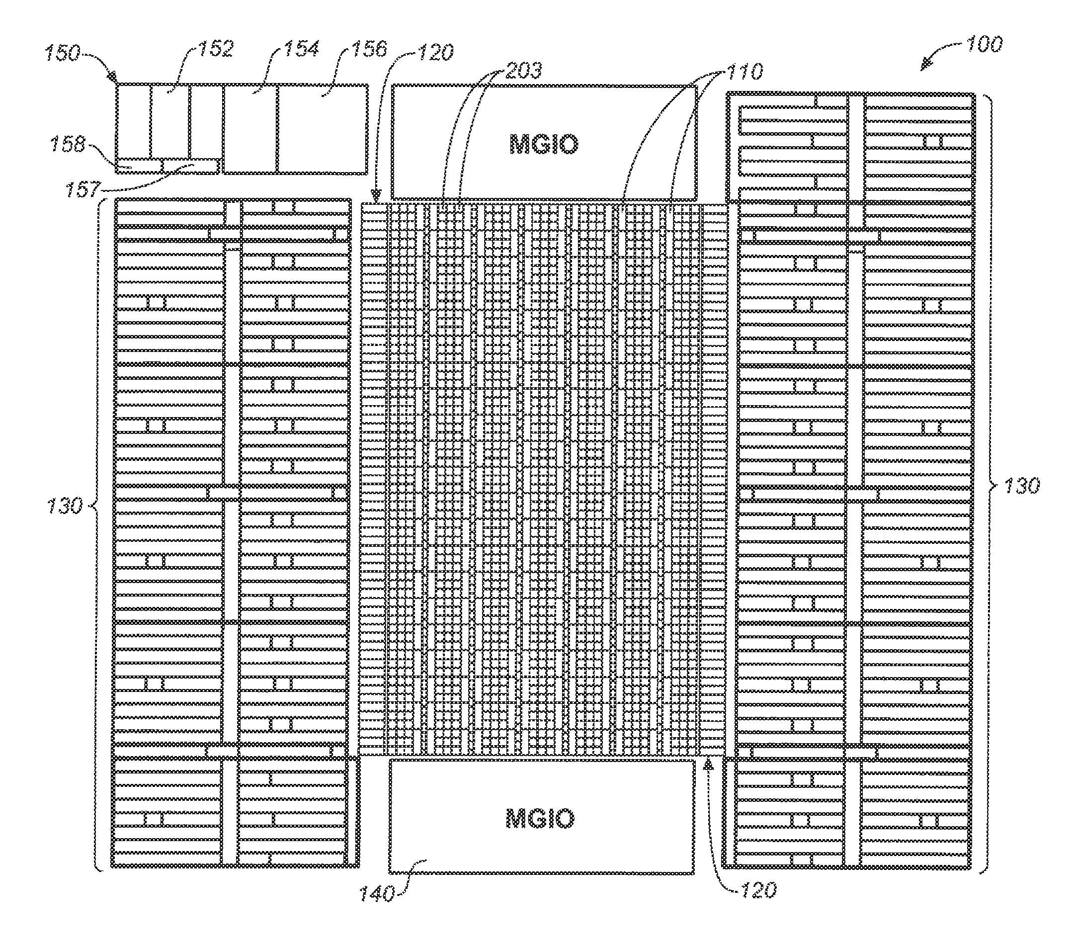
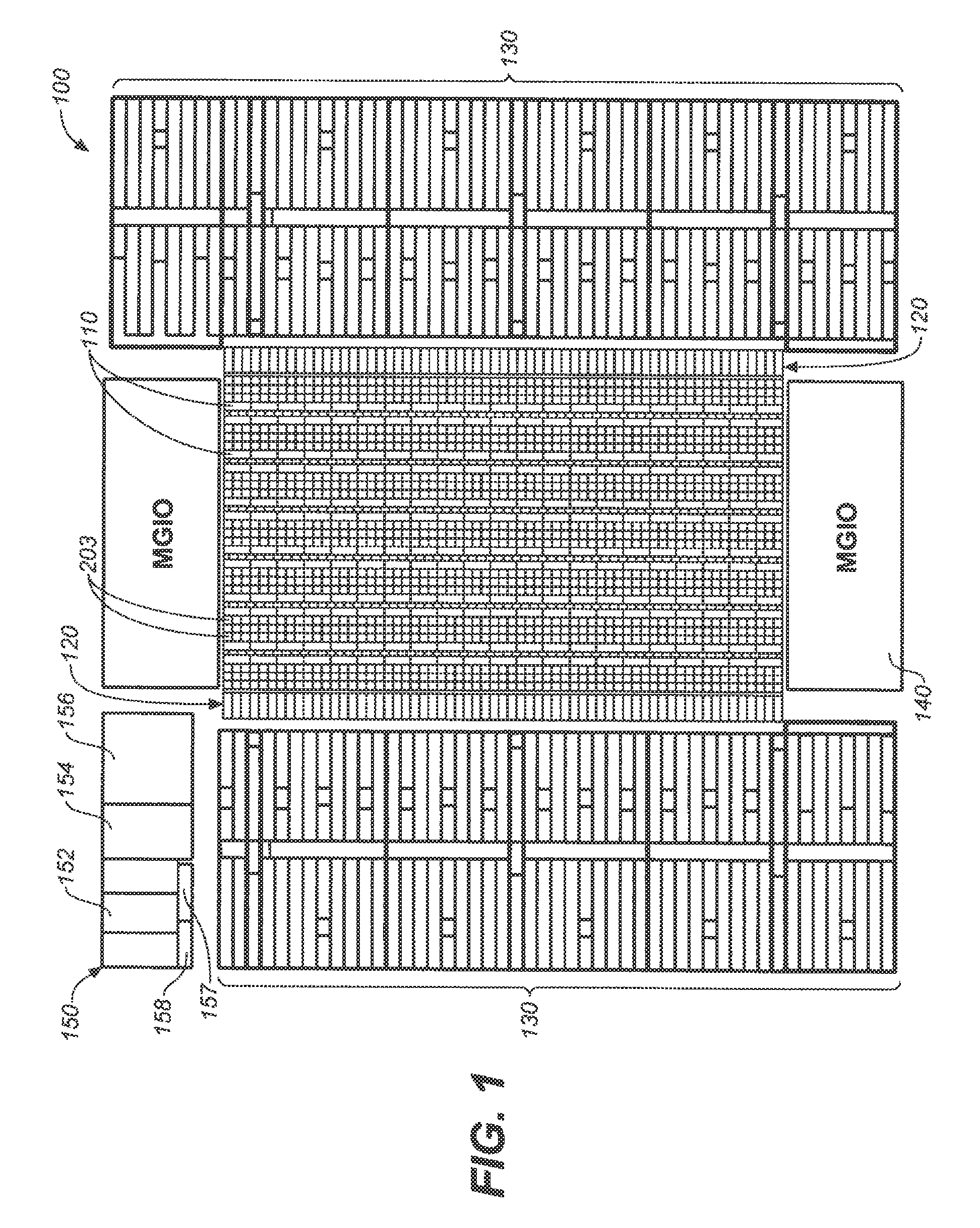
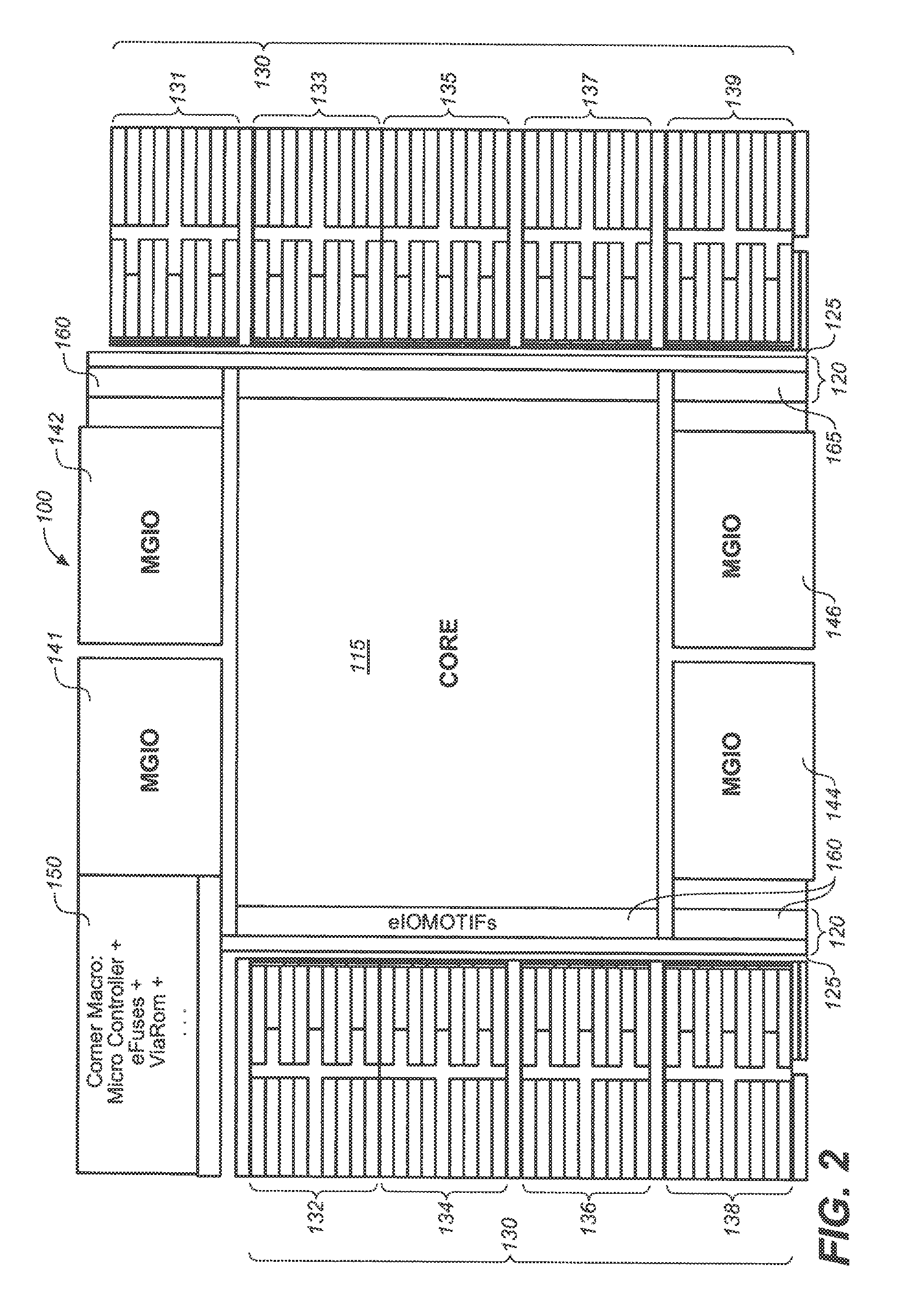
[0073]According to an embodiment of the invention, there in shown in FIGS. 1 and 2, not to scale, a generalized floor plan architecture of the Structured ASIC chip 100, code-named the RUBY architecture, a Structured ASIC having some pre-made elements that are mask-program...


PUM


Abstract

A floorplan for a Structured ASIC chip is shown having a core region containing memory and VCLB logic cells surrounded by a plurality of IO connection fabrics that include a first IO connection fabric comprising IO sub-banks connecting the core of the chip to pins for external signals to the core, a first high-speed routing fabric disposed along the east-west vertical top of the core and connects the core to high-speed IO such as SerDes; a network-aware connection fabric connects the core to a microcontroller primarily for testing and repair of the memory in the core; and a second-high speed routing fabric is disposed on the north-south vertical sides of the core and communicates with the IO sub-banks. The VCLB Structured ASIC chip is manufactured on a 28 nm CMOS process lithographic node or smaller, having several metal layers and preferably is programmed on a single via layer.

Description

CROSS-REFERENCE TO RELATED APPLICATIONS[0001]The present application is related to: U.S. application Ser. No. 13 / 49,510, for “VIA-CONFIGURABLE HIGH-PERFORMANCE LOGIC BLOCK INVOLVING TRANSISTOR CHAINS” by Alexander Andreev, Sergey Gribok, Ranko Scepanovic, Phey-Chuin TAN, Chee-Wei KUNG, filed the same day as the present invention, Oct. 11, 2012; U.S. application Ser. No. 13 / 649,547, for “CLOCK NETWORK FISHBONE ARCHITECTURE FOR A STRUCTURED ASIC MANUFACTURED ON A 28 NM CMOS PROCESS LITHOGRAPHIC NODE” by Alexander Andreev, Andrey Nikishin, Sergey Gribok, Phey-Chuin TAN, Choon-Hun CHOO, filed the same day as the present invention, Oct. 11, 2012; U.S. application Ser. No. 13 / 649,551, for “MICROCONTROLLER CONTROLLED OR DIRECT MODE CONTROLLED NETWORK-FABRIC ON A STRUCTURED ASIC” by Alexander Andreev, Andrey Nikitin, Marian Serbian, Massimo Verita, filed the same day as the present invention, Oct. 11, 2012; U.S. application Ser. No. 13 / 649,563 for “TEMPERATURE CONTROLLED STRUCTURED ASIC MAN...

Claims


Application Information

Patent Timeline
Patent Type & Authority Patents(United States)
IPC IPC(8): H03K19/177G06F17/50H03K19/0185
CPCH03K19/018585G06F17/505H01L2924/0002H01L2924/00G06F30/327
Inventor ANDREEV, ALEXANDERSCEPANOVIC, RANKO L.PAVISIC, IVANYAHONTOV, ALEXANDERUDOVIKHIN, MIKHAILVIKHLIANTSEV, IGORLIM, CHONG-TEIKLEE, SEOW-SUNGKUNG, CHEE-WEI
Owner INTEL CORP
Learn More