Method of minimizing charges accumulated at common electrode of display panel

a technology of display panel and common electrode, applied in the field of touch system, can solve problems such as adversely affecting the performance of the touch system

Active Publication Date: 2015-05-12
INNOLUX CORP +1
View PDF1 Cites 6 Cited by
  • Summary
  • Abstract
  • Description
  • Claims
  • Application Information

AI Technical Summary

Benefits of technology

[0007]When a mutual capacitance between a selected transmit electrode of the plurality of the transmit electrodes and a selected receive electrode of the plurality of the receive electrodes is measured, the voltage generating circuit applies a first voltage of a first polarity to the selected transmit electrode, and substantially concurrently applies a second voltage of a second polarity that is opposite to the first polarity to at least one other transmit electrode for minimizing charges associated with an application of the first voltage to the selected transmit electrode being accumulated at the first electrode.
[0008]The disclosure further discloses a method of minimizing the charges associated with the application of the first voltage. The method may include determining at least one of the transmit electrodes adjacent to a selected transmit electrode to which a first voltage of a first polarity is applied, when a mutual capacitance between the selected transmit electrode of the plurality of the transmit electrodes and a selected receive electrode of the plurality of the receive electrodes is measured, and substantially concurrently causing a second voltage of a second polarity opposite to the first polarity to be applied to the determined transmit electrode.

Problems solved by technology

However, charges corresponding to the sensing signals are coupled to the electrode of the display panel because of the presence of parasitic capacitances formed between the transmit electrodes and that particular electrode, which may adversely affect the performance of the touch system.

Method used


Image

  • Method of minimizing charges accumulated at common electrode of display panel
  • Method of minimizing charges accumulated at common electrode of display panel
  • Method of minimizing charges accumulated at common electrode of display panel

Examples


Embodiment Construction

[0015]The aforementioned illustrations and following detailed descriptions are exemplary for the purpose of further explaining the scope of the disclosure. Other objectives and advantages related to the disclosure will be illustrated in the subsequent descriptions and appended drawings.

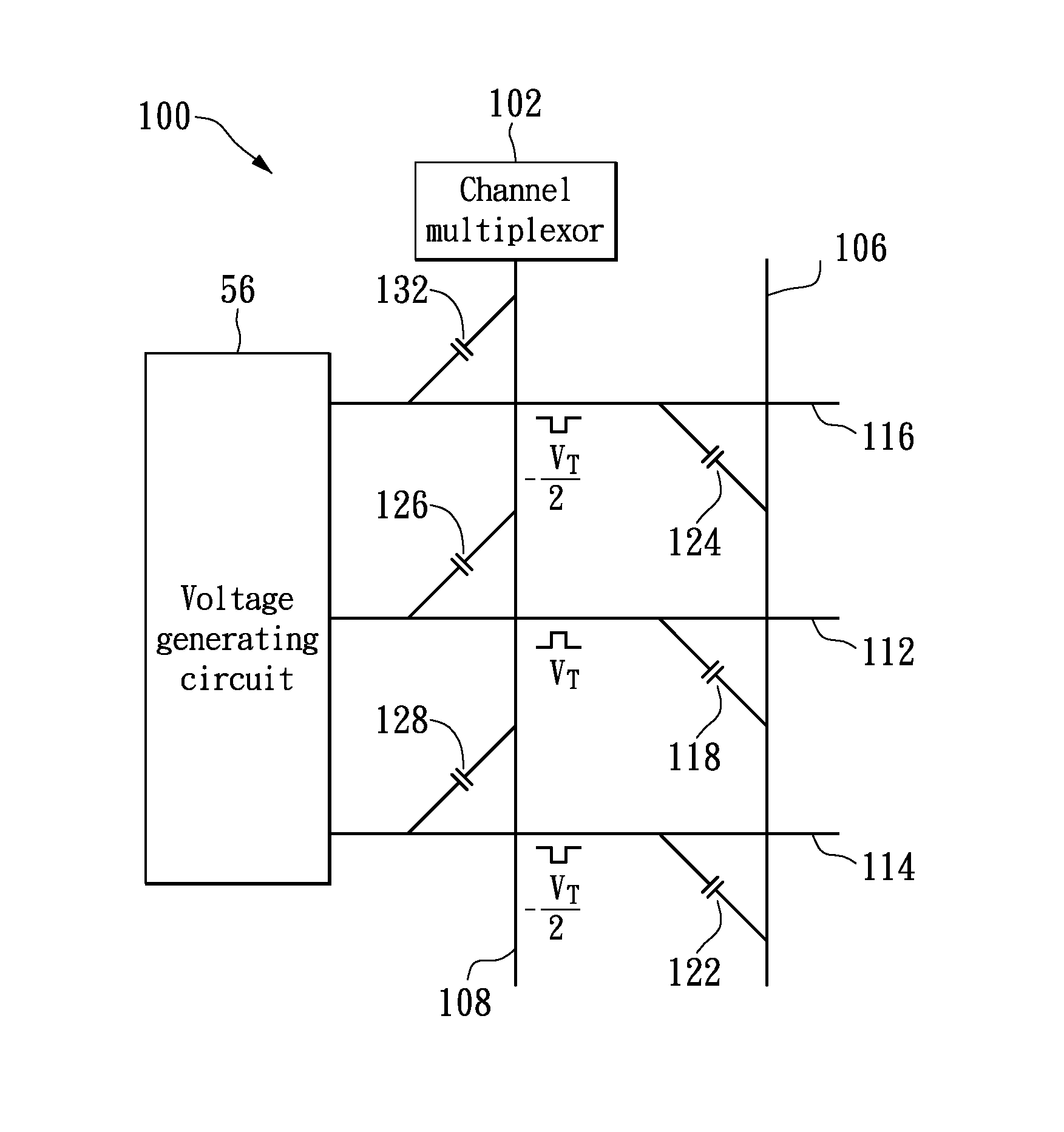
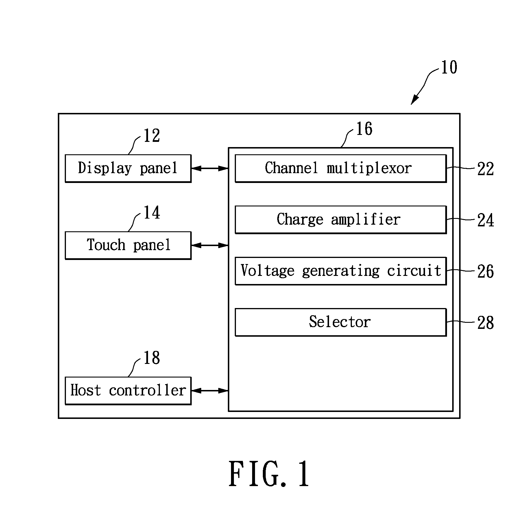
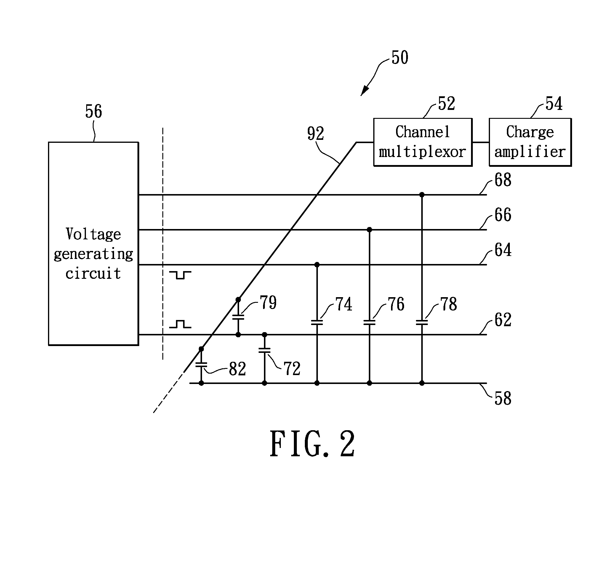
[0016]Please refer to FIG. 1 illustrating a simplified block diagram of a touch system 10 according to one embodiment of the disclosure. The touch system 10 may include a display panel 12, a touch panel 14, a driver module 16 for controlling operations of the display panel 12 and the touch panel 16, and a host controller 18 for controlling the driver module 16. The driver module 16 could be a touch display driver IC (DDI).

[0017]The driver module 16 may include a channel multiplexer 22 and a charge amplifier 24. The channel multiplexer 22 may be configured to multiplex signals resulting from the touch input and output a resulting sense output signal to the charge amplifier 24. Upon receiving the result...


PUM


Abstract

A touch system including a display panel associated with a first electrode, a touch panel having a plurality of touch electrodes having a plurality of transmit electrodes and a plurality of receive electrodes, and a voltage generating circuit is provided. When a mutual capacitance between a selected transmit electrode and a selected receive electrode is measured, the voltage generating circuit applies a first voltage of a first polarity to the selected transmit electrode, and substantially concurrently applies a second voltage of a second polarity that is opposite to the first polarity to at least one other transmit electrode for minimizing charges associated with an application of the first voltage to the selected transmit electrode and accumulated at the first electrode.

Description

BACKGROUND OF THE INVENTION[0001]1. Field of the Invention[0002]The disclosure relates to a touch system utilizing a mutual capacitive method for touch position detection, and more particularly, to a method of minimizing charges accumulated at an electrode associated with a display panel of the touch system when a touch position on a touch panel of the touch system is detected.[0003]2. Description of Related Art[0004]For detecting the touch position on the touch panel having a plurality of transmit electrodes, sensing signals, which could be predetermined voltage pulses, are typically employed to be applied to the transmit electrodes in a predetermined sequence. And charges corresponding to the sensing signals (or the applied voltage pulses) are collected by receive electrodes of the touch panel, creating multiple electrical fields. At the time a touch input on the touch panel is received, capacitances in the touch panel would vary as the result of changes in the electrical fields b...

Claims


Application Information

Patent Timeline
Patent Type & Authority Patents(United States)
IPC IPC(8): G06F3/041G06F3/044
CPCG06F3/044G06F3/04166G06F3/0446
Inventor EDWARDS, MARTINAYRES, RICHARD
Owner INNOLUX CORP
Why Eureka
Try Eureka