Insulated gate bipolar transistor

Active Publication Date: 2019-04-11
HITACHI ENERGY SWITZERLAND AG
View PDF0 Cites 3 Cited by
  • Summary
  • Abstract
  • Description
  • Claims
  • Application Information

AI Technical Summary

Benefits of technology

[0012]The inventive device integrates both active trench and well layers separated from the metal emitter electrode in a dummy cell as a single structure in order to achieve improved controllability performance while maintaining the advantages of reduced on-state and switching losses and improved blocking of the P-well trench IGBT cell. In the inventive design the dummy well layer is only capacitive coupled to the emitter potential and the coupling is weakened by the introduction of a thick insul

Problems solved by technology

The trench design, however, suffers from lower blocking capability near the bottom corners of the trenches due to high peak electric fields.
Therefore, the prior art device as shown in FIG. 1 results in bad controllability and high switching losses.
Furthermore, the high cell densities in trench designs will result in high short circuit currents.
However, such trenches are difficult to process and will still suffer from bad controllability.
However, such devices result in bad blocking properties and high switching losses due to slow field spreading from the pitched area during switc

Method used


Image

  • Insulated gate bipolar transistor
  • Insulated gate bipolar transistor
  • Insulated gate bipolar transistor

Examples


Embodiment Construction

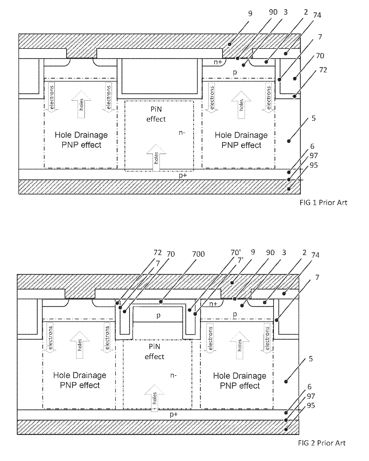
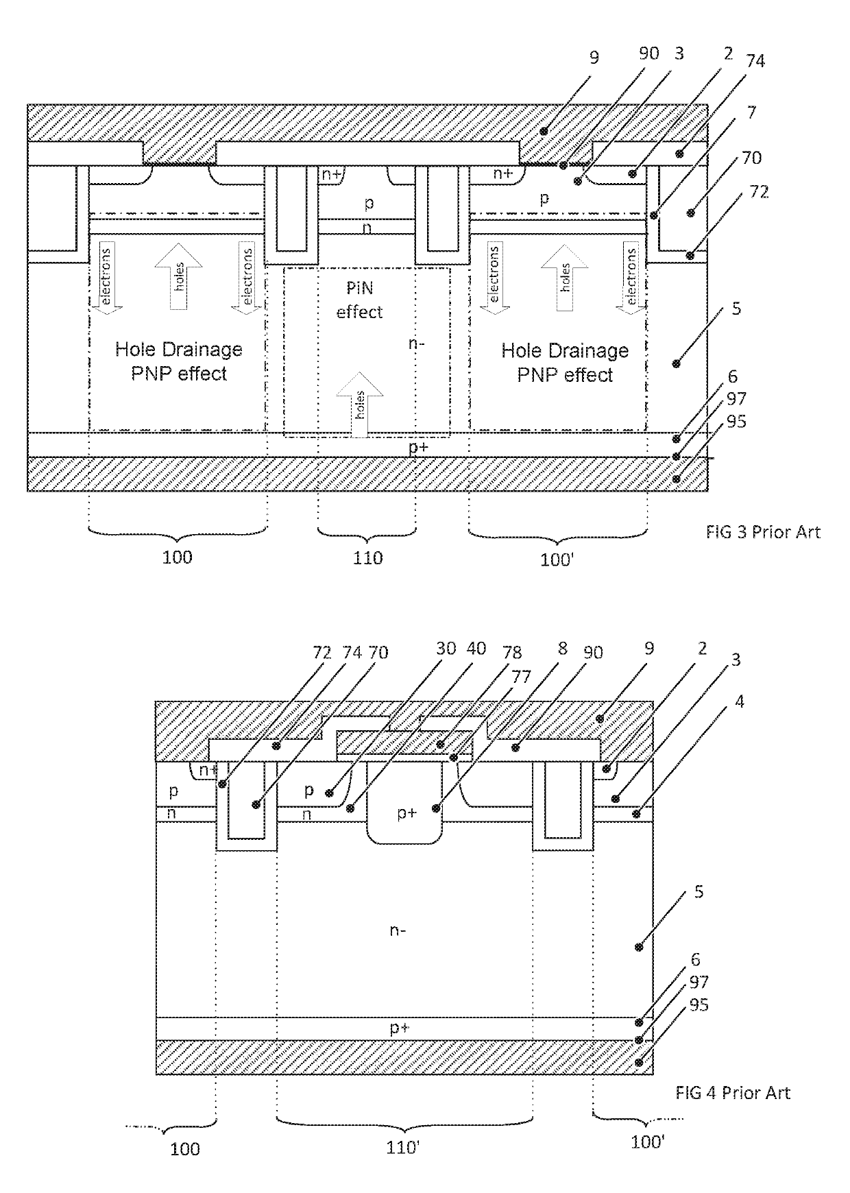
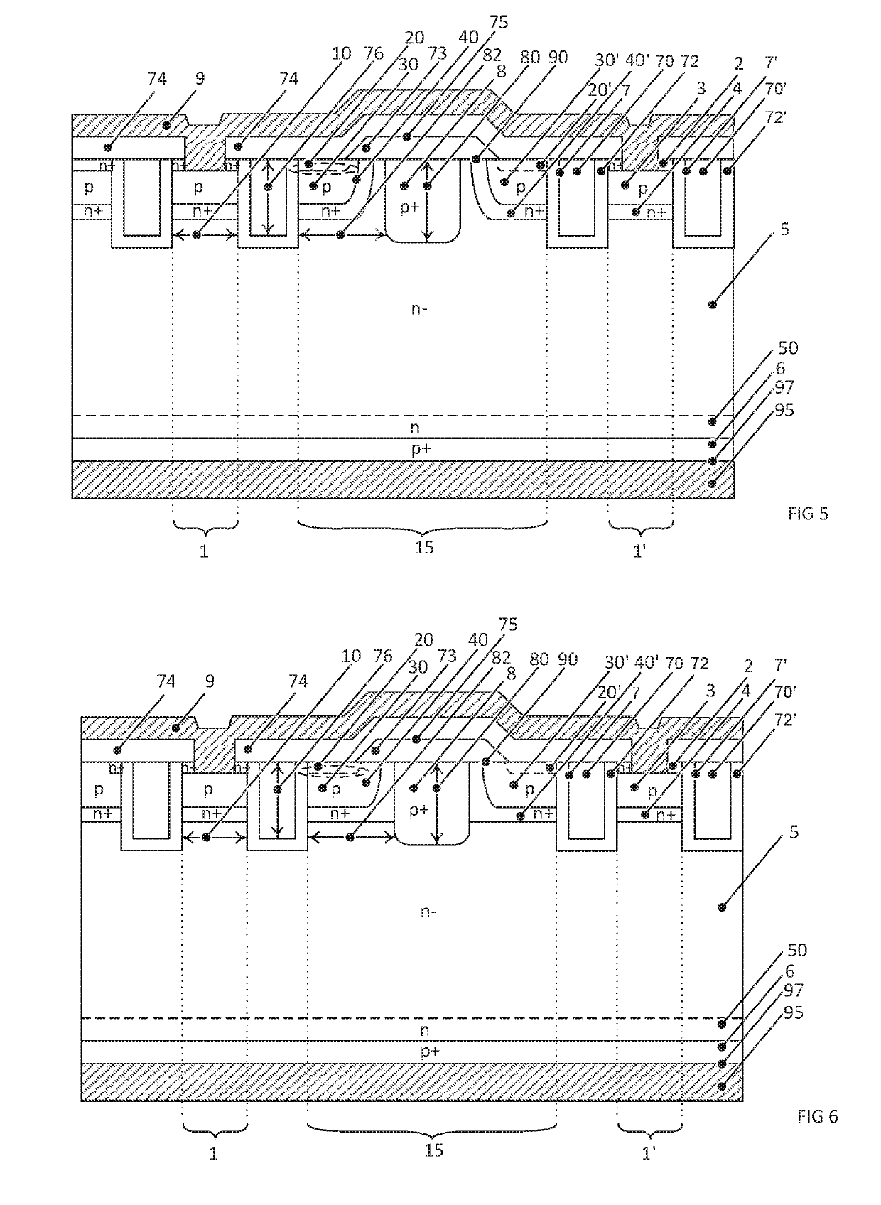
[0011]It is an object of the invention to provide a power semiconductor device with improved controllability. The problem is solved by the semiconductor device with the characteristics of claim 1.

[0012]The inventive device integrates both active trench and well layers separated from the metal emitter electrode in a dummy cell as a single structure in order to achieve improved controllability performance while maintaining the advantages of reduced on-state and switching losses and improved blocking of the P-well trench IGBT cell. In the inventive design the dummy well layer is only capacitive coupled to the emitter potential and the coupling is weakened by the introduction of a thick insulating layer stack with low capacitance in the dummy region. In addition the presence of the further enhancement layer, having a much larger doping concentration than the drift region, for separating the well from the trench gate electrode in the dummy region, further reduces the amount of holes whic...


PUM


Abstract

An IGBT is provided comprising at least two first cells (1, 1′), each of which having an n doped source layer (2), a p doped base layer (3), an n doped enhancement layer (4), wherein the base layer (3) separates the source layer (2) from the enhancement layer (4), an n− doped drift layer (5) and a p doped collector layer (6). Two trench gate electrodes (7, 7′) are arranged on the lateral sides of the first cell (1, 1′).
The transistor comprises at least one second cell (15) between the trench gate electrodes (7, 7′) of two neighboured first cells (1, 1′), which has on the emitter side (90) a p+ doped well (8) and a further n doped enhancement layer (40, 40′) which separates the well (8) from the neighboured trench gate electrodes (7, 7′). An insulator layer stack (75) is arranged on top of the second cell (15) on the emitter side (90) to insulate the second cell (15) and the neighboured trench gate electrodes (7, 7′) from the metal emitter electrode (9), which consists of a first insulating layer (73) and a second insulating layer (74), wherein the insulator stack (75) has a thickness on top of the well (8) of a first layer thickness plus the second insulating layer thickness and a thickness on top of the gate layer (70, 70′) of the second insulating layer thickness, wherein each thickness of the first insulating layer (73) and the second insulating layer (74) is at least 700 nm.

Description

FIELD OF INVENTION[0001]The invention relates to the field of power semiconductor devices. It relates to an Insulated Gate Bipolar according to the preamble of claim 1.BACKGROUND OF THE INVENTION[0002]Prior art IGBTs having trench MOS cells designs as shown in FIG. 1 have a trench gate electrode 7 with a gate layer 70, which is electrically insulated from a p doped base layer 3, an n+ doped source layer 2 and an n− doped drift layer 5 by a gate insulating layer 72. The trench gate electrode 7 is arranged in the same plane and lateral to the base layer 3 and extends deeper into the drift layer 5 than the base layer 3.[0003]With such trench gate electrode designs, the on-state losses are lower than for planar gate designs, because the trench design offers a vertical MOS channel, which provides enhanced injection of electrons in the vertical direction and suffers from no drawbacks from charge spreading (so called JFET effect) near the cell. Therefore the trench cells show much improved...

Claims


Application Information

Patent Timeline
IPC IPC(8): H01L29/739H01L29/06H01L29/10H01L29/40H01L21/265H01L21/266H01L21/225H01L21/324H01L29/66
CPCH01L29/7397H01L29/0696H01L29/1095H01L29/1083H01L29/408H01L21/26513H01L21/266H01L21/2253H01L21/324H01L29/66348H01L29/0603H01L29/66325H01L29/7393H01L29/402H01L29/0619
Inventor CORVASCE, CHIARAKOPTA, ARNOSTANDENNA, MAXIRAHIMO, MUNAF
Owner HITACHI ENERGY SWITZERLAND AG
Why Eureka
Try Eureka