Integrated micro-plasma limiter

a micro-plasma limiter and integrated technology, applied in the direction of limiting amplitude without controlling loop, emergency protective circuit arrangement, waveguide type devices, etc., can solve the problems of significant signal loss before the signal can be amplified, integrated circuits can be susceptible to high intensity or high power signals, and the low noise amplifiers (lna) provided immediately behind the antenna at the front end of the receiver can be destroyed

Active Publication Date: 2015-06-09
NORTHROP GRUMMAN SYST CORP
View PDF27 Cites 0 Cited by
  • Summary
  • Abstract
  • Description
  • Claims
  • Application Information

AI Technical Summary

Problems solved by technology

Integrated circuits can be susceptible to high intensity or high power signals, such as electromagnetic pulses (EMP), whether they be unintended random signals or intentional hostile signals.
Particularly, low noise amplifiers (LNA) provided immediately behind the antenna at the front end of a receiver can be destroyed if the antenna receives a high intensity power signal, where the power susceptibility of the LNA becomes more sensitive to incoming power as the frequency and noise performance of the receiver increases.
Known plasma power limiters are typically separate bulky devices provided at the front end of the receiver or other circuit that cause significant signal loss before the signal can be amplified for further processing.
Therefore, for some applications the design of the specific circuit would not allow for such a power limiter to be incorporated.

Method used


Image

  • Integrated micro-plasma limiter
  • Integrated micro-plasma limiter
  • Integrated micro-plasma limiter

Examples


Embodiment Construction

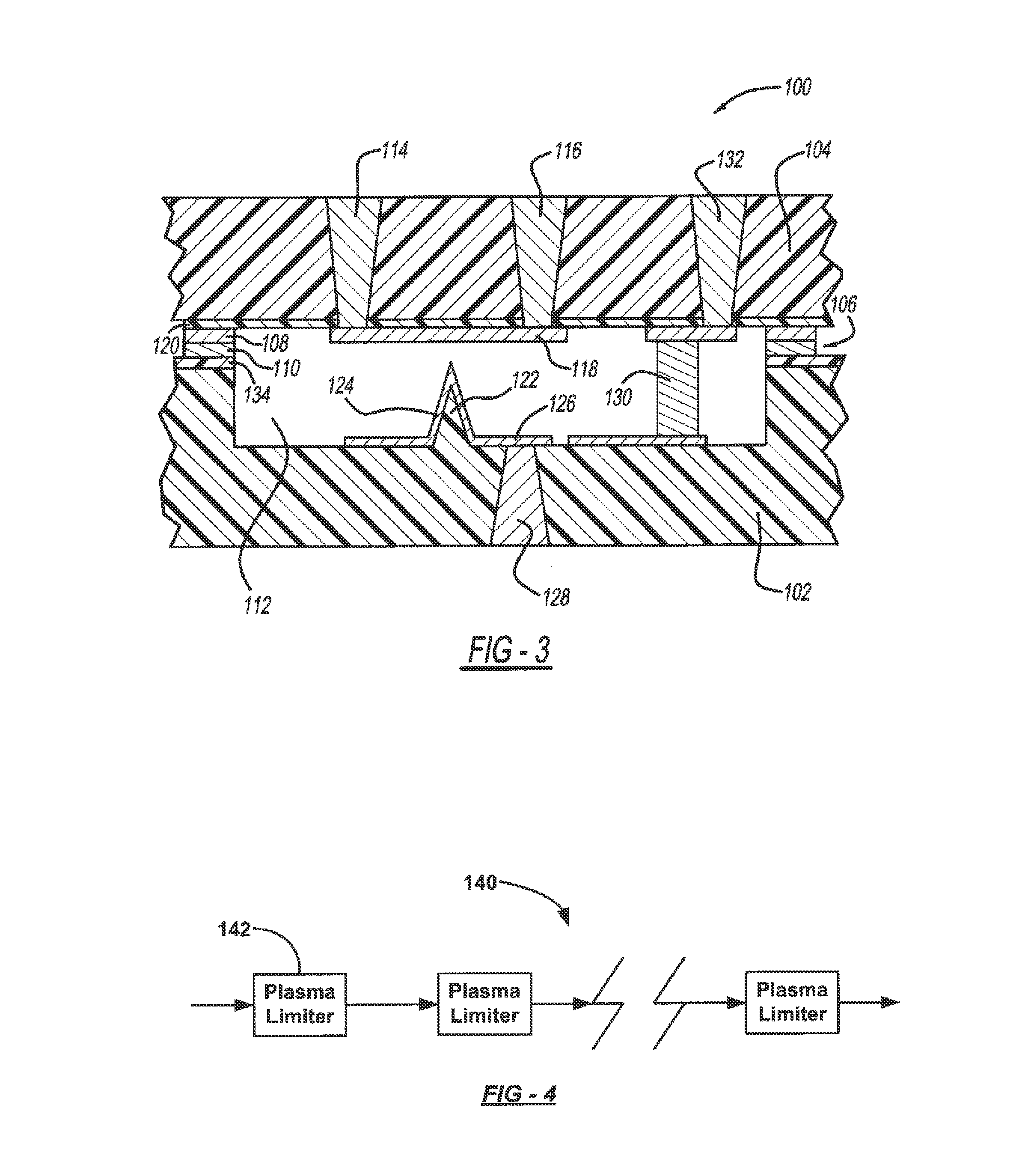
[0013]The following discussion of the embodiments of the invention directed to an integrated wafer-level plasma power limiter is merely exemplary in nature, and is in no way intended to limit the invention or its applications or uses. For example, the discussion herein is directed to the plasma limiter being employed in the front end of a receiver. However, as will be appreciated by those skilled in the art, the plasma power limiter discussed herein can be used in any suitable circuit that includes electronics that could be damaged by high intensity signals.

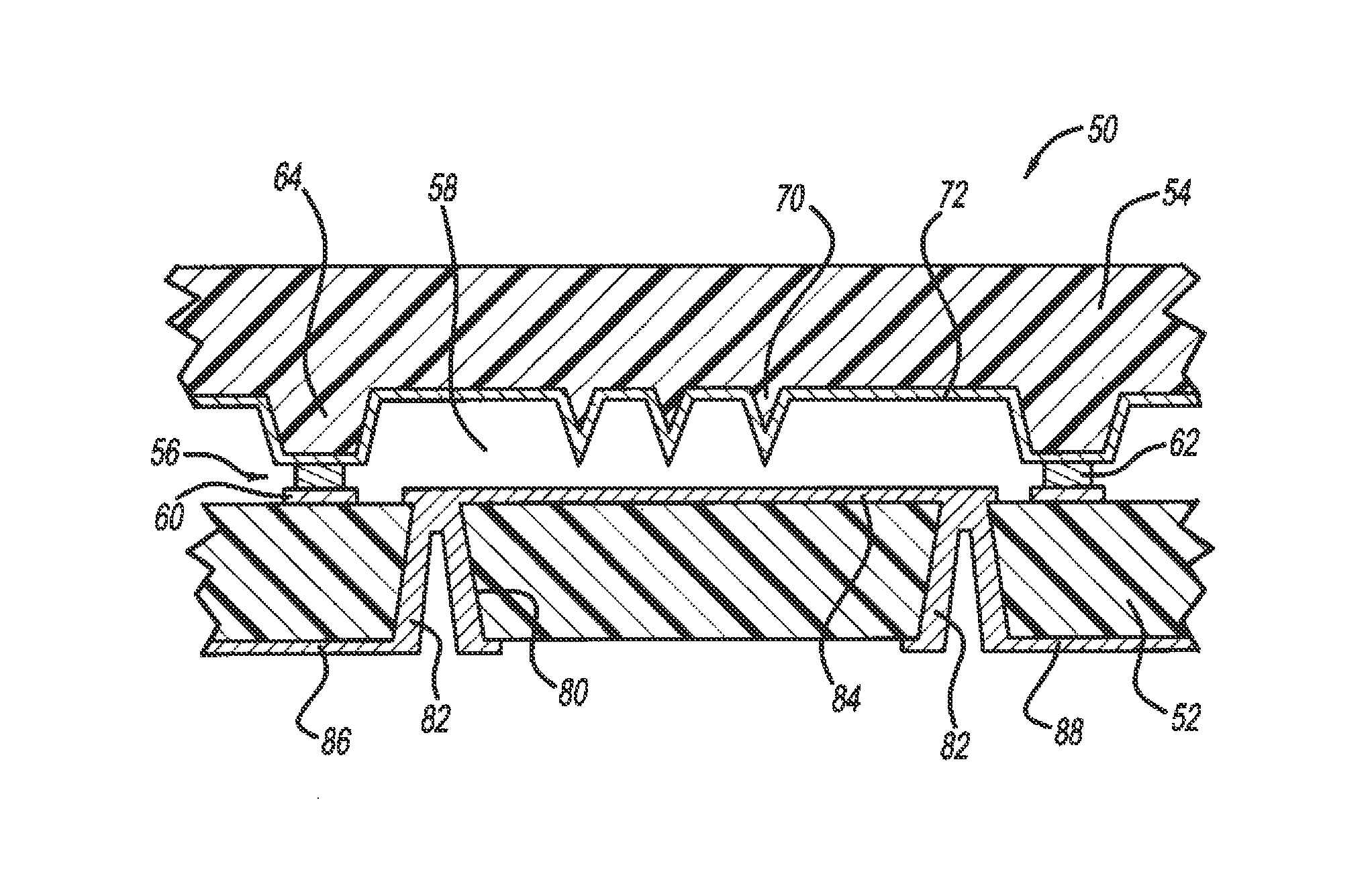
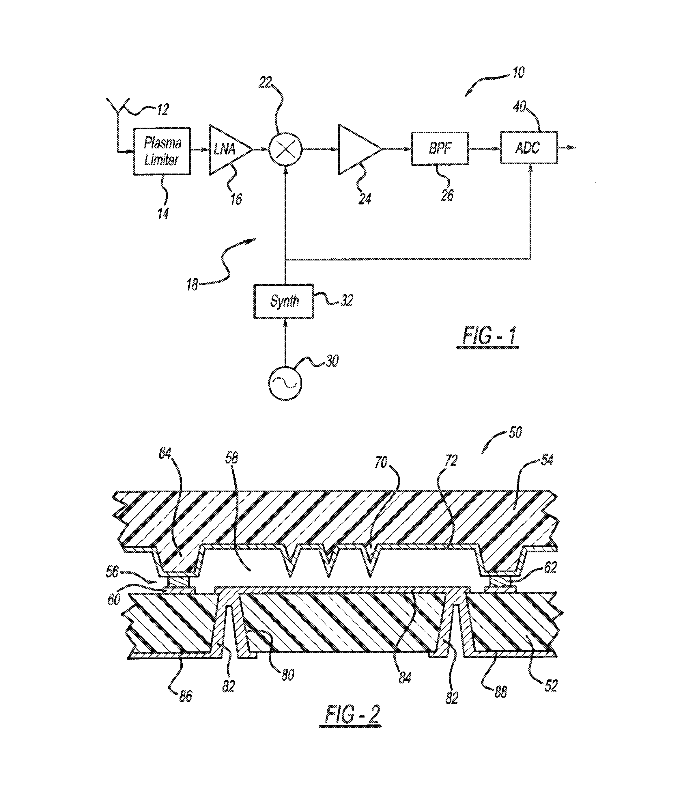
[0014]FIG. 1 is a simple schematic block diagram of a front end of a receiver 10 that could have many applications, such as wireless communication applications. The receiver 10 is intended to represent any receiver operated at any desirable frequency and being responsive to signals from any suitable source. The receiver 10 includes an antenna 12 that receives the signals to be processed by the receiver 10. The antenna 12 can be a...


PUM


Abstract

A plasma power limiter fabricated using wafer-level fabrication techniques with other circuit elements. The plasma limiter includes a signal substrate and a trigger substrate defining a hermetically sealed cavity therebetween in which is encapsulated an ionizable gas. The signal substrate includes a signal line within the cavity and the trigger substrate includes at least one trigger probe extending from the trigger substrate towards the transmission line. If a signal propagating on the transmission line exceeds a power threshold, the gas within the cavity is ionized creating a conduction path between the transmission line and the trigger probe that draws off the high power current.

Description

CROSS-REFERENCE TO RELATED APPLICATIONS[0001]This application claims the benefit of the filing date of provisional application Ser. No. 61 / 653,840 titled, Integrated Micro-Plasma Limiter, filed May 31, 2012.BACKGROUND[0002]1. Field[0003]This invention relates generally to a plasma power limiter and, more particularly, to a plasma power limiter that is monolithically fabricated using wafer-level processing so as to be integrated on the same wafer as other circuits.[0004]2. Discussion of the Art[0005]It is known in the art to provide wafer-level packaging for integrated circuits, such as monolithic millimeter-wave integrated circuits (MMIC), formed on substrate wafers. In one wafer-level packaging design, a cover wafer is mounted to the substrate wafer using a bonding ring so as to provide a hermetically sealed cavity in which the integrated circuit is provided. Typically, many integrated circuits are formed on the substrate wafer and covered by a single cover wafer, where each integr...

Claims


Application Information

Patent Timeline
Patent Type & Authority Patents(United States)
IPC IPC(8): H01T4/16H03G11/00H01P1/14H01L23/60
CPCH01T4/16H03G11/002H03G11/004H01P1/14H01L23/60H01L2924/0002H01L2924/00
Inventor CHANG-CHIEN, PATTYHENNIG, KELLY JILLZENG, XIANGLINYANG, JEFFREY M.
Owner NORTHROP GRUMMAN SYST CORP
Why Eureka
Try Eureka