Current detector allowing a large supply voltage range
a current detector and supply voltage technology, applied in the field of integrated circuits, can solve the problems of difficult to reach supply voltage and electrical consumption
- Summary
- Abstract
- Description
- Claims
- Application Information
AI Technical Summary
Benefits of technology
Problems solved by technology
Method used
Image

Examples
Embodiment Construction
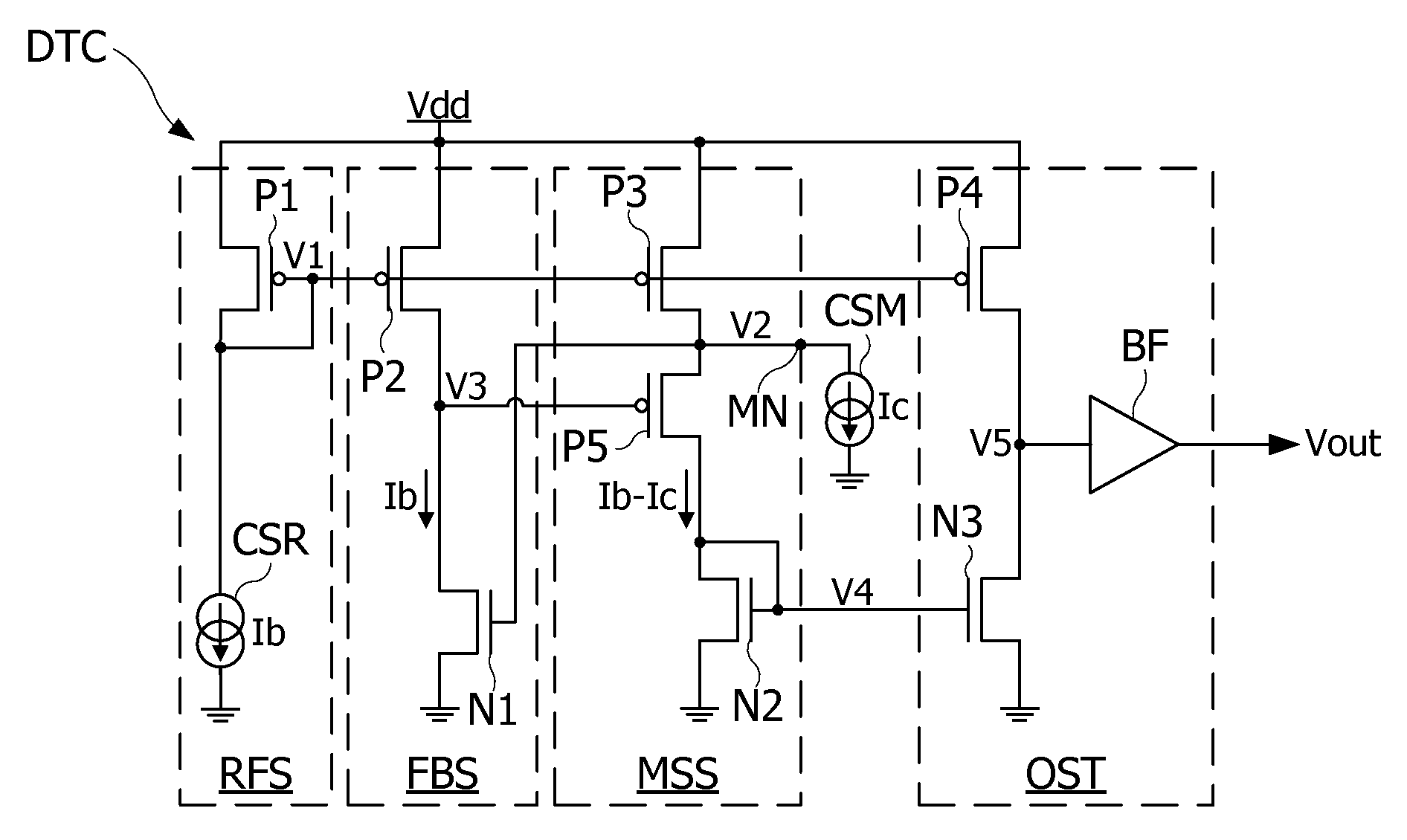
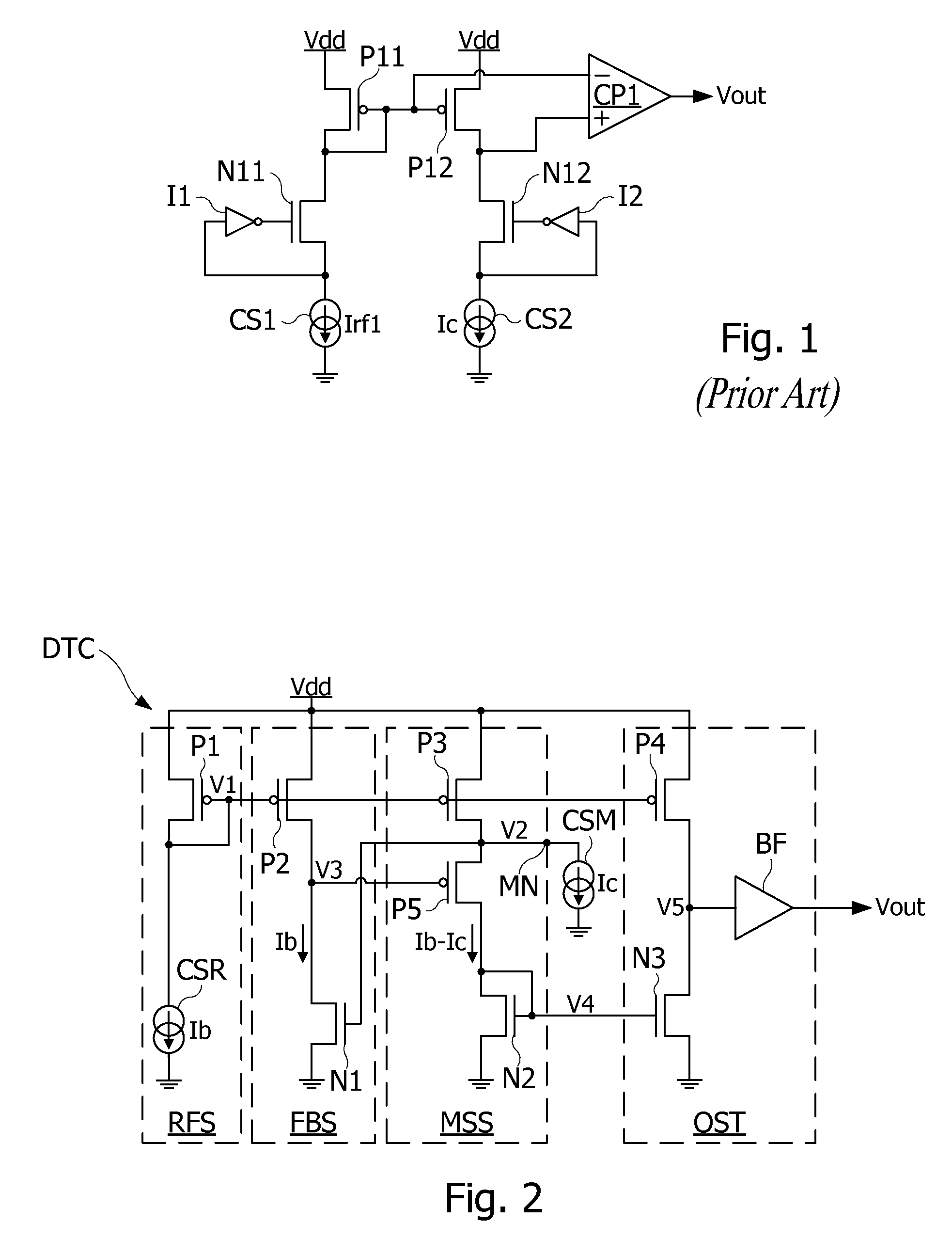
[0029]FIG. 2 shows a current detection circuit DTC, according to one embodiment. The circuit DTC comprises a reference stage RFS, a feedback stage FBS, a measurement stage MSS, and an output stage OST. The reference stage RFS comprises a P-channel MOS transistor, referred to as P1, and a bias current source CSR. Transistor P1 comprises a source terminal receiving a supply voltage Vdd of the circuit, and gate and drain terminals connected to the ground through current source CSR. The current source CSR is configured to generate a substantially constant bias current Ib independent of possible variations of the supply voltage Vdd. However, the current Ib may vary as a function of the circuit operating temperature and the circuit manufacture conditions.
[0030]The feedback stage FBS comprises a P-channel MOS transistor, referred to as P2, and an N-channel MOS transistor, referred to as N1, these two transistors forming an amplifier. Transistor P2 comprises a source terminal receiving the ...
PUM
 Abstract
Description
Claims
Application Information
 - R&D
- Intellectual Property
- Life Sciences
- Materials
- Tech Scout
- Unparalleled Data Quality
- Higher Quality Content
- 60% Fewer Hallucinations
Browse by: Latest US Patents, China's latest patents, Technical Efficacy Thesaurus, Application Domain, Technology Topic, Popular Technical Reports.
© 2025 PatSnap. All rights reserved.Legal|Privacy policy|Modern Slavery Act Transparency Statement|Sitemap|About US| Contact US: help@patsnap.com