
Electronic device and method for generating a curvature compensated bandgap reference voltage

a technology of curvature compensation and reference voltage, which is applied in the direction of electric variable regulation, process and machine control, instruments, etc., can solve the problems of difficult design and manufacture of low cost and highly accurate reference in digital cmos processes, affecting the stability of the base-emitter voltage of a bipolar transistor over temperature, and not necessarily providing the most accurate devices. , to achieve the effect of less sensitive to process variations

Active Publication Date: 2015-08-11
TEXAS INSTR INC
View PDF13 Cites 9 Cited by
  • Summary
  • Abstract
  • Description
  • Claims
  • Application Information

AI Technical Summary

Benefits of technology

[0008]It is an object of the invention to provide an electronic device or a method generating a bandgap reference voltage which is more accurate, less sensitive to process variations and production spread without being more expensive or complex than the prior art.
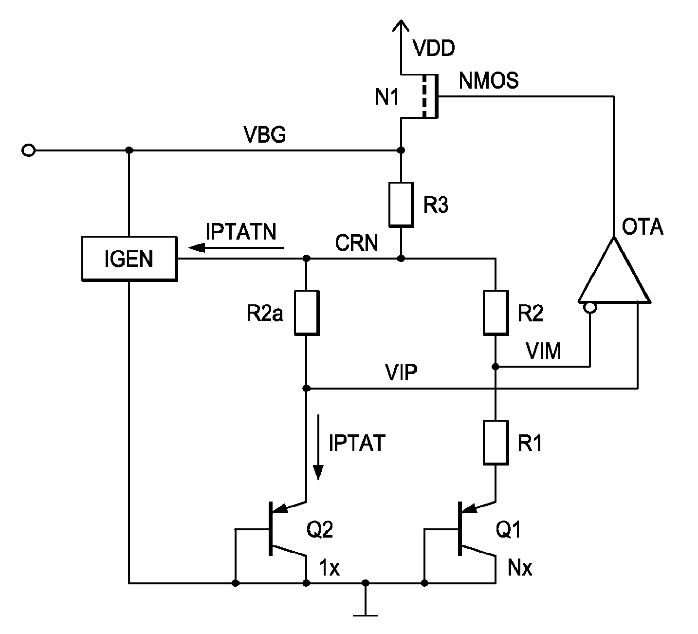
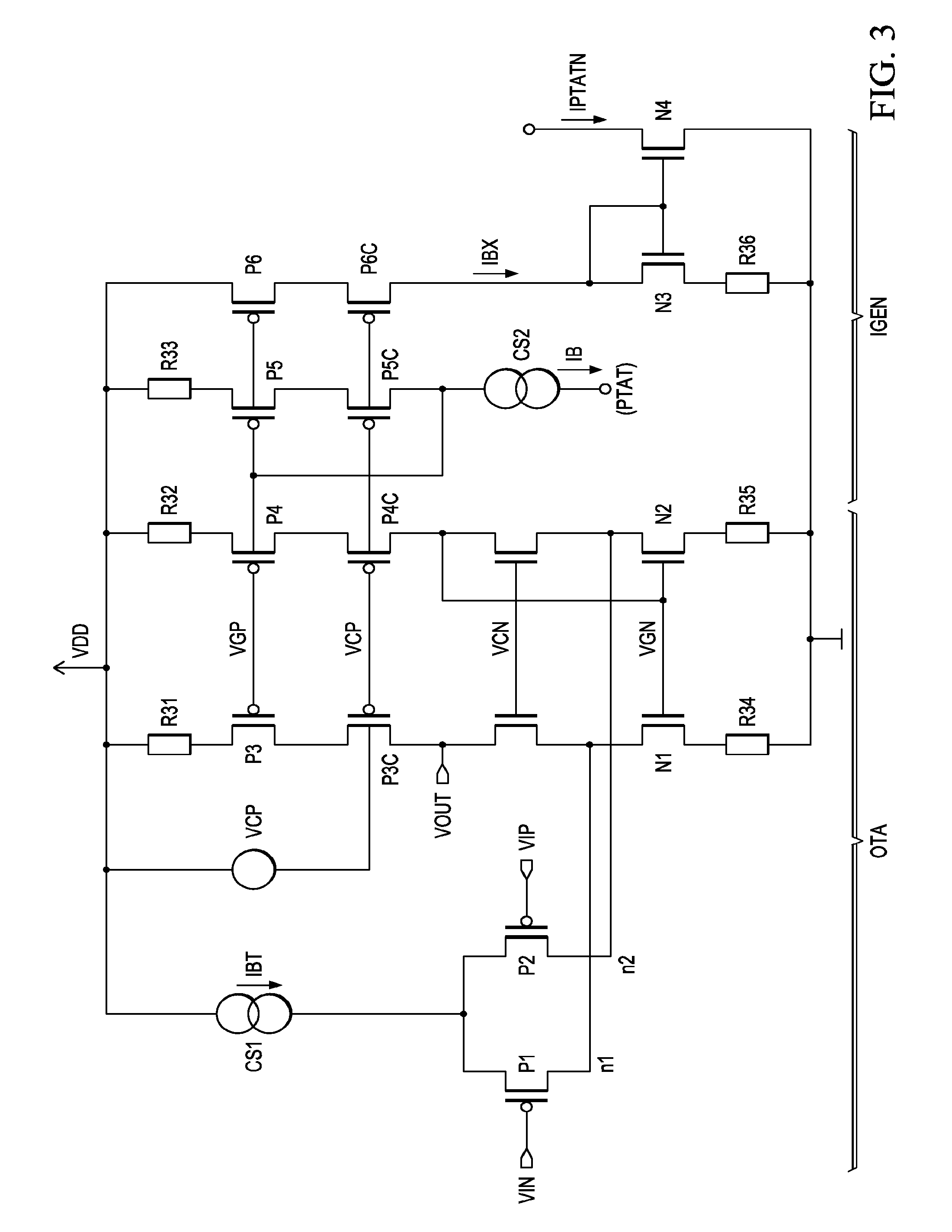
[0013]The curvature compensation stage is preferably a translinear current mode circuit. A translinear current mode circuit is inherently stable and accurate and can be easily implemented as an add-on to the amplifier. Translinear current mode circuits are suitable to implement higher order functions of voltages or currents. The translinear current mode circuit may include a mismatched current mirror. In a preferred embodiment, the translinear current mode circuit supplies a non-linear compensation current through the first or second bipolar transistor (such as the collector current) which varies with temperature according to the third power of the temperature.
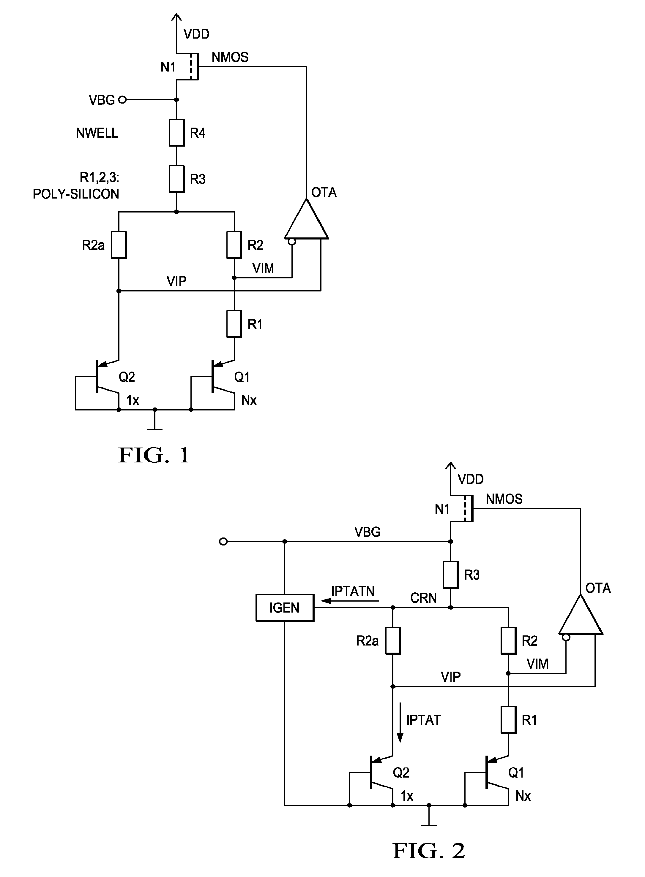
[0014]Mismatch may be achieved using resistors in the curvature compensation stage. The resistors may advantageously be of the same type as the other resistors in the bandgap reference generator. This avoids using resistors of a different type, such as the NWELL transistor in prior art solutions. The curvature compensation stage can use the same devices as the remainder of the bandgap reference generator (for example MOS transistors and poly-silicon resistors, except for the first bipolar transistor and the second bipolar transistor). The curvature compensation current then depends on gate oxide thickness only. This is usually well controlled in CMOS technologies. Process variations of the resistance values of the resistors affect the bandgap core, the curvature compensation stage and the amplifier. The negative effects cancel each other out and reduce the effects of process variation.

Problems solved by technology

The design and manufacture of low cost and highly accurate references in digital CMOS processes is difficult.
Thus a trimming procedure does not necessarily provide the most accurate devices.
The base-emitter voltage of a bipolar transistor is not absolutely stable over temperature.
This generally results from non-linear temperature behavior of the BJT saturation current.
This NWELL sheet resistance it fairly difficult to control in known CMOS or BICMOS technologies and renders VBE curvature compensation less robust than required.

Method used


Image

  • Electronic device and method for generating a curvature compensated bandgap reference voltage
  • Electronic device and method for generating a curvature compensated bandgap reference voltage
  • Electronic device and method for generating a curvature compensated bandgap reference voltage

Examples


Embodiment Construction

[0023]FIG. 2 illustrates a simplified circuit diagram of a bandgap reference generator with a VBE curvature compensation according to an embodiment of the invention.

[0024]There are two current paths. The first path includes a first bipolar transistor Q1 and two series resistors R1 and R2. Resistors R1 and R2 may be poly-silicon resistors. Both the base and the collector of Q1 are coupled to ground. The second current path includes a second bipolar transistor Q2. The second transistor Q2 also has both its base and collector coupled to ground. This connection of transistors Q1 and Q2 are due to restrictions of the technology used for implementing the electronic device. A typical CMOS technology forms the electronic device as an integrated semiconductor electronic device. The emitter area of Q1 is N times the emitter area of Q2. Resistor R1 has one terminal coupled to the emitter of Q1 and other terminal coupled to R2. The node between R1 and R2 is VIM. Resistor R2a has one terminal co...


PUM


Abstract

The invention relates to an electronic device with a bandgap reference generator including a first path with series connection of a first bipolar transistor, a first resistor and a second resistor, and a second path with series connection of a second bipolar transistor and a third resistor. The first and second paths are supplied current via a common node through a fourth resistor controlled by an amplifier sensing voltage drops within the first and second paths. A curvature compensation stage compensates for a variation of base emitter voltage of the bipolar transistors by drawing a compensation current from the common resistor node.

Description

CLAIM OF PRIORITY[0001]This application claims priority under 35 U.S.C. 119(s) to German Patent Application No. 10 2010 007 771.2 filed Feb. 12, 2010.TECHNICAL FIELD OF THE INVENTION[0002]The technical field of this invention is an electronic device and method for generating a curvature compensated bandgap reference voltage.BACKGROUND OF THE INVENTION[0003]Accurate analog-to-digital converters are needed which for various applications needing very exact reference voltages having low temperature drift. The design and manufacture of low cost and highly accurate references in digital CMOS processes is difficult. Providing test flow on automatic test equipment (ATE) is another important aspect of manufacturing these electronic devices. Production trimming is expensive and should avoided whenever possible. A typical test procedure includes only two test insertions at two temperatures. The lower temperature is generally not the minimum operating temperature of the device. Thus a trimming ...

Claims


Application Information

Patent Timeline
Patent Type & Authority Patents(United States)
IPC IPC(8): G05F3/16G05F3/30
CPCG05F3/30G05F3/16G05F3/267
Inventor ARNOLD, MATTHIAS
Owner TEXAS INSTR INC
Learn More