

Display substrate including an auxiliary electrode
a technology of auxiliary capacitors and substrates, applied in the field of substrates, can solve the problems of multi-domain techniques involving cost and/or aperture ratio, bad side visibility, etc., and achieve the effects of minimizing thickness of protecting layers, maximizing capacitance of auxiliary capacitors, and advantageously reducing the thickness of protecting layers
- Summary
- Abstract
- Description
- Claims
- Application Information
AI Technical Summary
Benefits of technology
Problems solved by technology
Method used
Image

Examples
Embodiment Construction
[0030]Hereinafter, the present invention will be explained in detail with reference to the accompanying drawings.
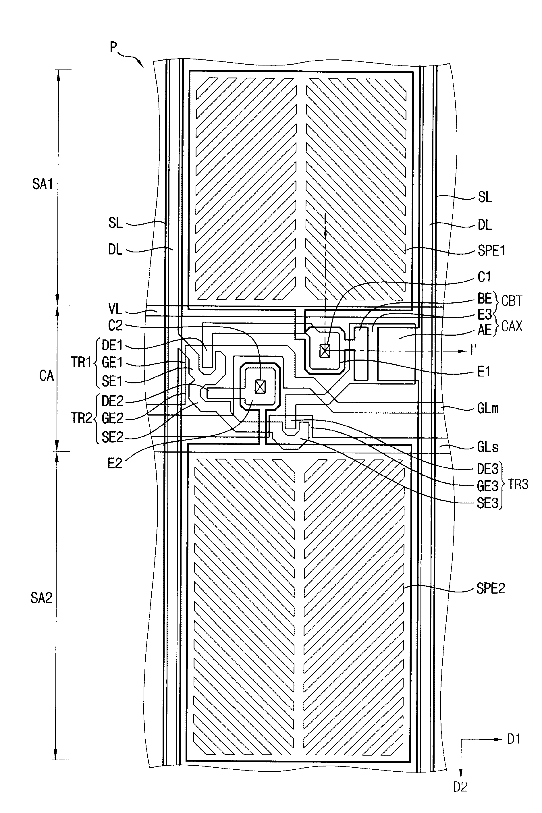
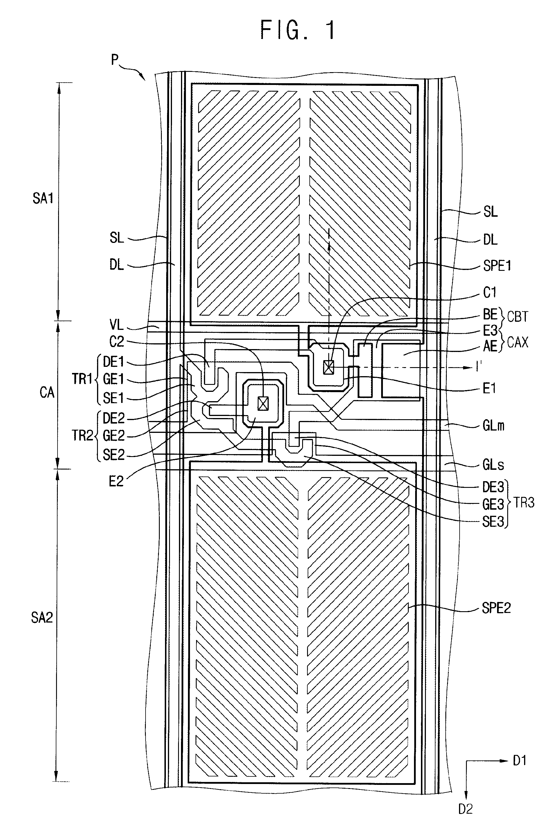
[0031]FIG. 1 is a plan view illustrating a display panel according to one or more embodiments of the present invention.
[0032]Referring to FIG. 1, the display panel includes a main gate line GLm, a secondary gate line GLs, a voltage line VL, a data line DL, a shielding line SL, and a pixel P. The pixel P includes a first switching element TR1, a first sub-pixel electrode SPE1, a second switching element TR2, a second sub-pixel electrode SPE2, a third switching element TR3, a boosting capacitor CBT, and an auxiliary capacitor CAX.
[0033]The main gate line GLm may extend in a first direction D1; the main gate line GLm and other main gate lines (associated with other pixels of the display panel) may be arranged along a second direction D2 different from (e.g., substantially perpendicular to) the first direction D1. The main gate line GLm is electrically connected to the first ...
PUM
| Property | Measurement | Unit |
|---|---|---|
| capacitance | aaaaa | aaaaa |
| capacitance | aaaaa | aaaaa |
| capacitance | aaaaa | aaaaa |
Abstract
Description
Claims
Application Information