Method for driving a liquid crystal display device, an array substrate, method of manufacturing the array substrate and liquid crystal display device having the same

a liquid crystal display and array substrate technology, applied in the direction of electric digital data processing, instruments, computing, etc., can solve the problems of many defects in the manufacturing process of multi-cell gap lcd devices, alignment defects such as polyimide agglomeration, texture defects may occur, etc., to increase the transmittance of the transmissive electrode, reduce the number of steps of the manufacturing process, and increase the contrast ratio

Active Publication Date: 2015-09-29
TCL CHINA STAR OPTOELECTRONICS TECH CO LTD
View PDF17 Cites 0 Cited by
  • Summary
  • Abstract
  • Description
  • Claims
  • Application Information

AI Technical Summary

Benefits of technology

[0009]Example embodiments of the present invention provide a method for driving a liquid crystal display (LCD) device for preventing contrast ratio reduction and texture defects.
[0010]Example embodiments of the present invention also provide an array substrate for preventing contrast ratio reduction and texture defects.
[0020]In an example embodiment of the present invention, the first and the second boost lines may be formed on both sides of the gate line on the substrate and substantially parallel to the gate line. The gate line may extend between the first and the second switching elements. The first and the second boost lines, the gate line, the first and the second source electrodes, and the second drain electrode may be formed under the reflective electrode for increasing transmittance of the transmissive electrode.
[0021]According to some example embodiments of the present invention, an LCD device is driven on a transflective mode with a mono-cell gap. Thus, the number of steps of a manufacturing process may be decreased, and contrast ratio may be increased. Also, textures and alignment defects caused by multi-cell gaps may be prevented. As a result, display quality may be improved and the yield of the LCD device may be increased. Thus, the present invention may be applied to the LCD device driven in a transflective mode with a mono-cell gap.

Problems solved by technology

However, the multi-cell gap LCD device may include many defects from a manufacturing process.
For example, alignment layer deposition defects caused by the steps of the reflective area, alignment defects such as polyimide agglomeration, and texture defects may occur.

Method used


Image

  • Method for driving a liquid crystal display device, an array substrate, method of manufacturing the array substrate and liquid crystal display device having the same
  • Method for driving a liquid crystal display device, an array substrate, method of manufacturing the array substrate and liquid crystal display device having the same
  • Method for driving a liquid crystal display device, an array substrate, method of manufacturing the array substrate and liquid crystal display device having the same

Examples


Embodiment Construction

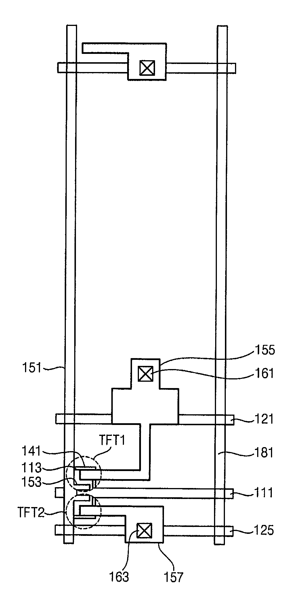
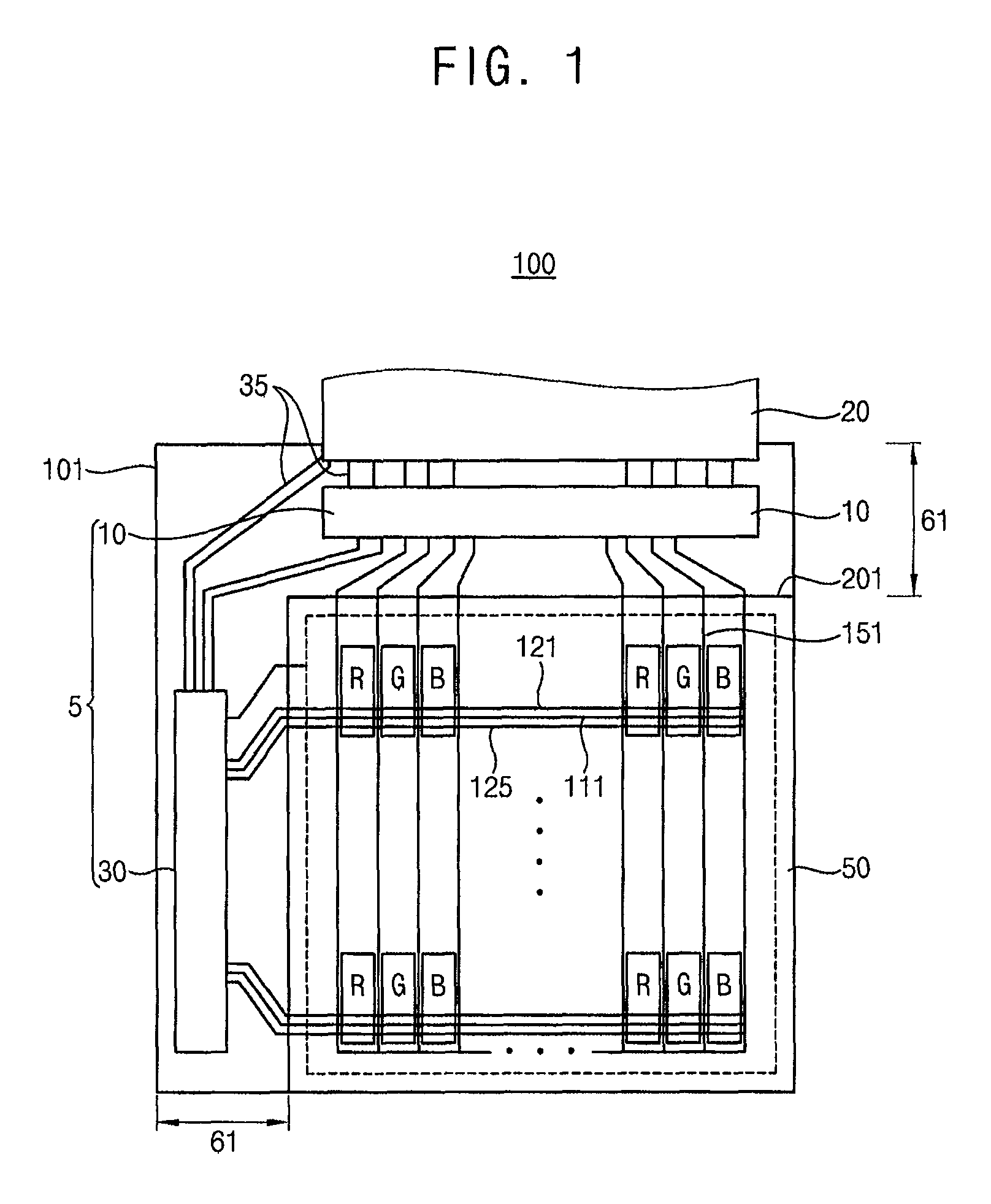
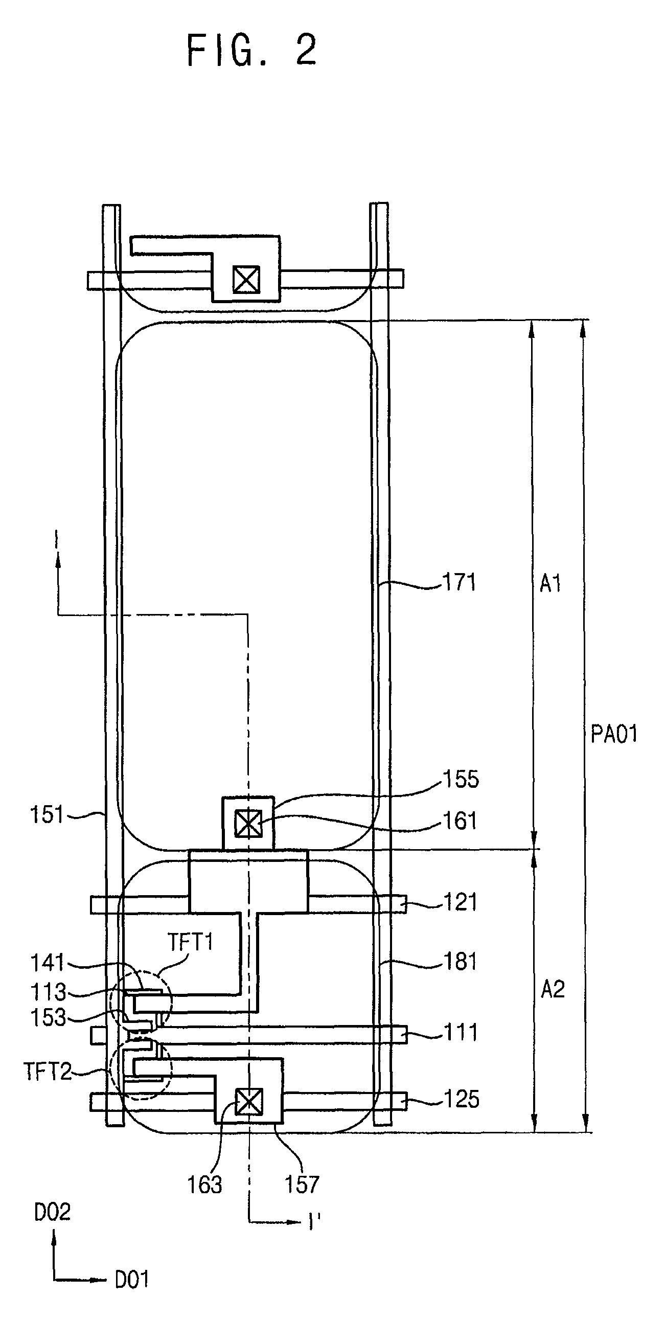
[0040]The present invention is described more fully hereinafter with reference to the accompanying drawings, in which example embodiments of the present invention are shown. The present invention may, however, be embodied in many different forms and should not be construed as limited to the example embodiments set forth herein. Rather, these example embodiments are provided so that this disclosure will be thorough and complete, and will fully convey the scope of the present invention to those skilled in the art. In the drawings, the sizes and relative sizes of layers and regions may be exaggerated for clarity.

[0041]It will be understood that when an element or layer is referred to as being “on,”“connected to” or “coupled to” another element or layer, it can be directly on, connected or coupled to the other element or layer or intervening elements or layers may be present. In contrast, when an element is referred to as being “directly on,”“directly connected to” or “directly coupled ...


PUM

PropertyMeasurementUnit
pixel voltageaaaaaaaaaa
voltageaaaaaaaaaa

Abstract

In a method for driving a liquid crystal display (LCD) device, an array substrate, a method of manufacturing the array substrate and the LCD device having the same, data signals are boosted by a first and a second boost signals up to a first and a second pixel voltages, respectively. The first and the second pixel voltages are applied to a transmissive electrode and a reflective electrode, respectively. As a result, the retardation of light passing through a liquid crystal layer on the transmissive electrode and the retardation of light of the liquid crystal layer on the reflective electrode may be controlled to be substantially equal to each other. Thus, the LCD device is driven in a transflective mode with a mono-cell gap so that the yield of the LCD device may be increased.

Description

PRIORITY STATEMENT[0001]This application claims priority under 35 U.S.C. §119 to Korean Patent Application No. 2008-59430, filed on Jun. 24, 2008 in the Korean Intellectual Property Office (KIPO), the contents of which are herein incorporated by reference in their entirety.BACKGROUND OF THE INVENTION[0002]1. Field of the Invention[0003]Example embodiments of the present invention relate to a method for driving a liquid crystal display (LCD) device, an array substrate, a method of manufacturing the array substrate, and an LCD device having the same. More particularly, example embodiments of the present invention relate to a method for driving an LCD device in a transflective mode with a mono-cell gap, an array substrate, a method of manufacturing the array substrate and an LCD device having the same.[0004]2. Description of the Related Art[0005]Generally, a liquid crystal display (LCD) device displays an image by controlling the transmittance of liquid crystal using an electric field....

Claims


Application Information

Patent Timeline
Patent Type & Authority Patents(United States)
IPC IPC(8): G02F1/1362G02F1/1368G09G3/36G02F1/1335
CPCG09G3/3648G02F1/13624G02F1/1368G02F1/133555G09G2300/0426G09G2300/0439G09G2300/0456G09G2300/0465G09G2300/0852G09G2320/0233G02F1/133G09G3/20G09G3/36
Inventor CHO, YONG-SEOKKIM, JAE-HYUNKIM, GEE-BUMHWANG, JAE-HOON
Owner TCL CHINA STAR OPTOELECTRONICS TECH CO LTD
Why Eureka
Try Eureka