Manufacturing method of liquid discharge head
a manufacturing method and liquid discharge technology, applied in the direction of coatings, pretreated surfaces, printing, etc., can solve the problem of similar manufacturing methods, and achieve the effect of hardly causing a variation in liquid discharge properties, excellent formation, and good shape precision
- Summary
- Abstract
- Description
- Claims
- Application Information
AI Technical Summary
Benefits of technology
Problems solved by technology
Method used
Image
Examples
embodiment 1
(Embodiment 1)
Manufacturing of Master Mold 1
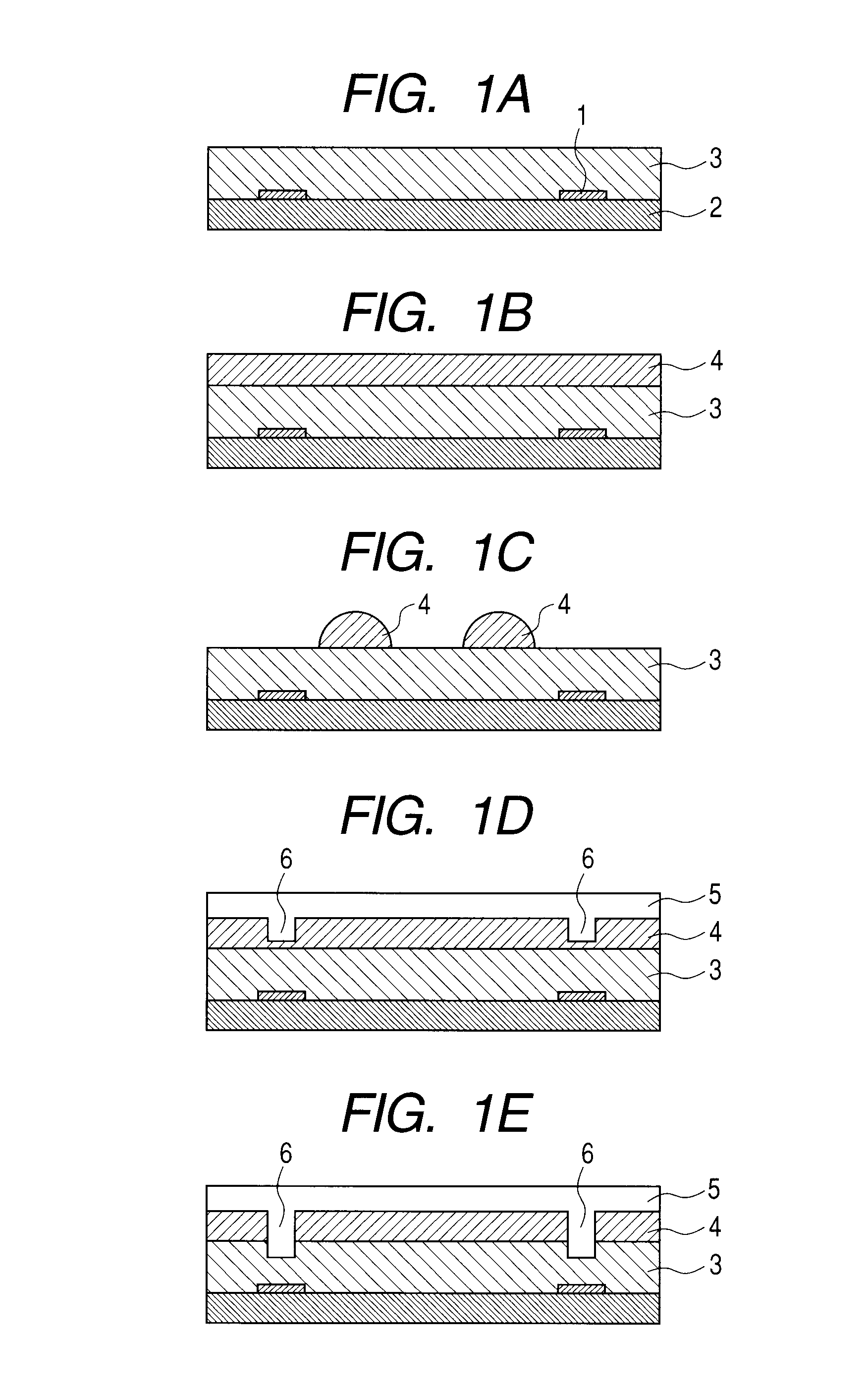
[0060]Firstly, a positive type resist, OFPR-800 (trade name) produced by Tokyo Ohka Kogyo Co., Ltd., was applied onto a quartz substrate. The quartz substrate was exposed to light using a mask of an ink discharge port pattern, and then developed. Subsequently, the surface of the substrate was etched by reactive ion etching (RIE) using the pattern of OFPR-800 as a mask to produce protrusions of the ink discharge port pattern, and then the OFPR-800 was separated from the substrate. At that time, the height of the protrusions of the ink discharge port pattern was about 10 μm.
[0061]Subsequently, an aluminum (Al) film was formed, by thermochemical vapor deposition (CVD), on the surface of the quartz substrate where the protrusions were formed. The quartz substrate was heated to 300° C., and trimethylaluminum (TMA) was used as a source gas. The Al film was formed on not only end surfaces and bottom surface of the quartz substrate but also on sid...
embodiment 2
(Embodiment 2)
Manufacturing of Inkjet Recording Head 1
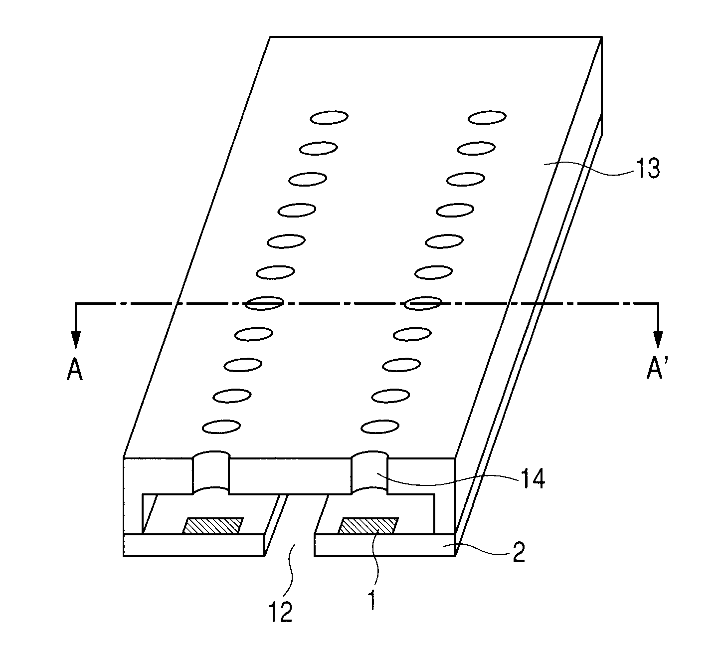
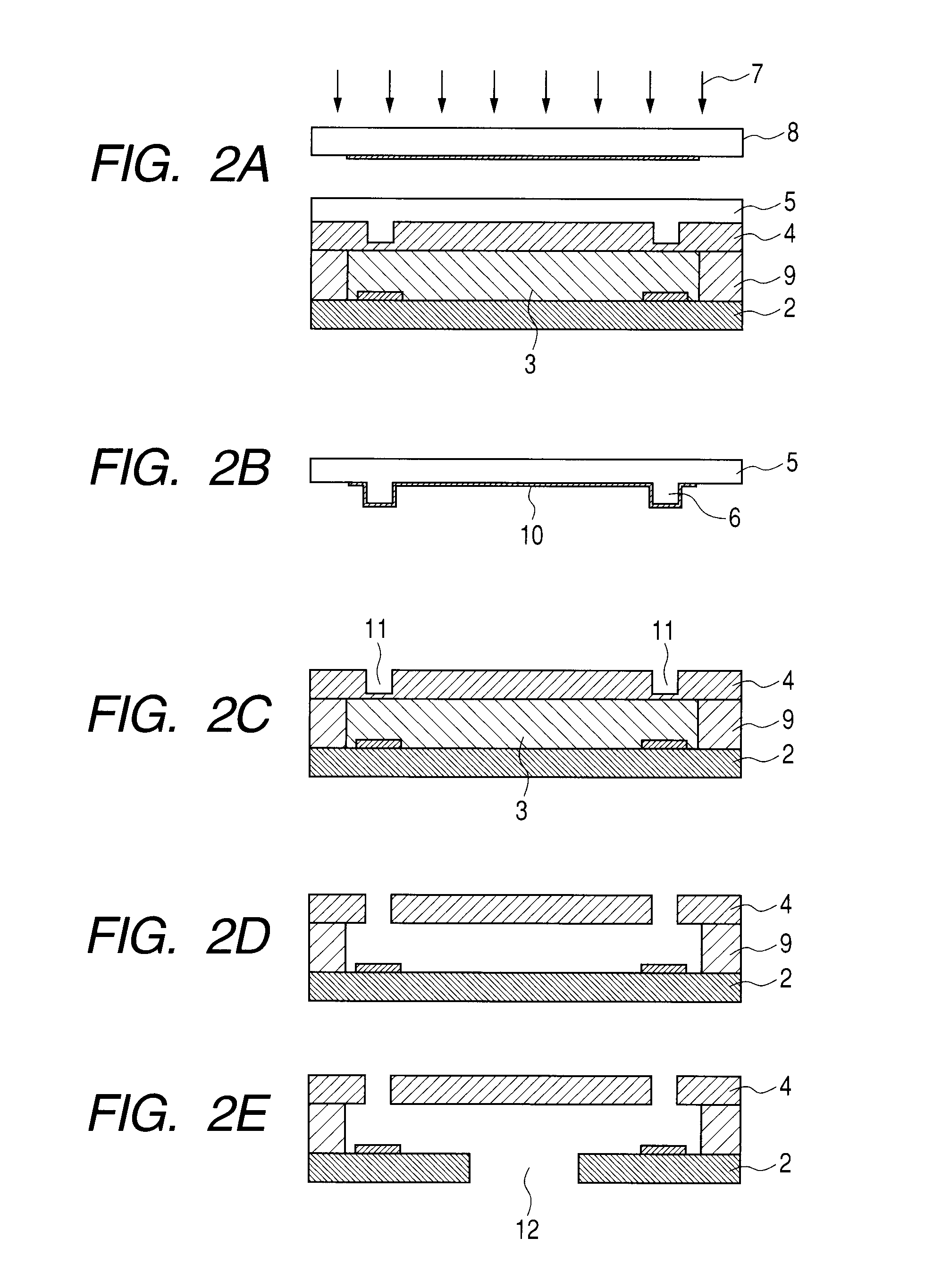
[0064]Firstly, an ink supply port was formed in a rear surface of a silicon substrate on which surface electro-thermal converting elements were formed as ink discharge energy generating elements. Specifically, a cyclized rubber resist was applied, as a protective film, onto the surface of the silicon substrate where the electro-thermal converting elements were formed. Subsequently, a silicon oxide which had been preliminarily formed on the rear surface of the silicon substrate was patterned, and using the patterned silicon oxide as a mask, the silicon substrate was immersed in a tetramethylammonium hydroxide aqueous solution (22%, 83° C.) for 16 hours. Then, the silicon substrate was subjected to anisotropic etching to form an ink supply port, and then the protective film was separated from the silicon substrate.
[0065]Next, SU-8 3025 (trade name) produced by MicroChem serving as a cationically photocurable resin was formed on a P...
embodiment 3
(Embodiment 3)
Manufacturing of Master Mold 2
[0073]Firstly, a positive type resist, OFPR-800 (trade name) produced by Tokyo Ohka Kogyo Co., Ltd., was applied onto a quartz substrate. The quartz substrate was exposed to light using a mask of an ink discharge port pattern, and then developed. Subsequently, the surface of the substrate was etched by reactive ion etching (RIE) using the pattern of OFPR-800 as a mask to produce protrusions of the ink discharge port pattern, and then the OFPR-800 was separated from the substrate. At that time, the height of protrusions of the ink discharge port pattern was about 10 μm.
PUM
| Property | Measurement | Unit |
|---|---|---|
| height | aaaaa | aaaaa |
| thickness | aaaaa | aaaaa |
| thickness | aaaaa | aaaaa |
Abstract
Description
Claims
Application Information


