Semiconductor equipment

a technology of semiconductors and equipment, applied in the direction of chemical vapor deposition coatings, electric discharge tubes, coatings, etc., can solve the problems of long maintenance time, unstable process, and affecting process yield, so as to reduce maintenance time and improve process results

Inactive Publication Date: 2016-02-23
HERMES EPITEK
View PDF9 Cites 2 Cited by
  • Summary
  • Abstract
  • Description
  • Claims
  • Application Information

AI Technical Summary

Benefits of technology

[0008]Accordingly, the present invention has been made in order to meet such a need described above, and it is an object of the present invention to provide a semiconductor equipment having cleaning function. The particles or contaminants accumulated within the reaction chamber can be timely removed so as to avoid excessive accumulation.
[0010]The semiconductor equipment of the present invention is capable of timely removing the particles accumulated within the liner device by the venting device. The venting device is capable of removing the particles within the liner device without opening the reaction chamber. Thus, the excessive accumulation of the particles within the reaction chamber can be avoided. Moreover, the maintenance time is decreased, and the process result is improved.

Problems solved by technology

Thus, process results and the process yields are affected by the residues.
Generally speaking, the particles or contaminants accumulated within the reaction chamber can be removed manually when the reaction chamber is opened; however, this usually leads to negative results, such as long maintenance times, unstable process results, and so on.

Method used


Image

  • Semiconductor equipment
  • Semiconductor equipment
  • Semiconductor equipment

Examples


Embodiment Construction

[0014]The detailed description of the present invention will be discussed in the following embodiments, which are not intended to limit the scope of the present invention and can be adapted for other applications. While drawings are illustrated in detail, it is appreciated that the quantity of the disclosed components may be greater or less than that disclosed, except when expressly restricting the amount of the components.

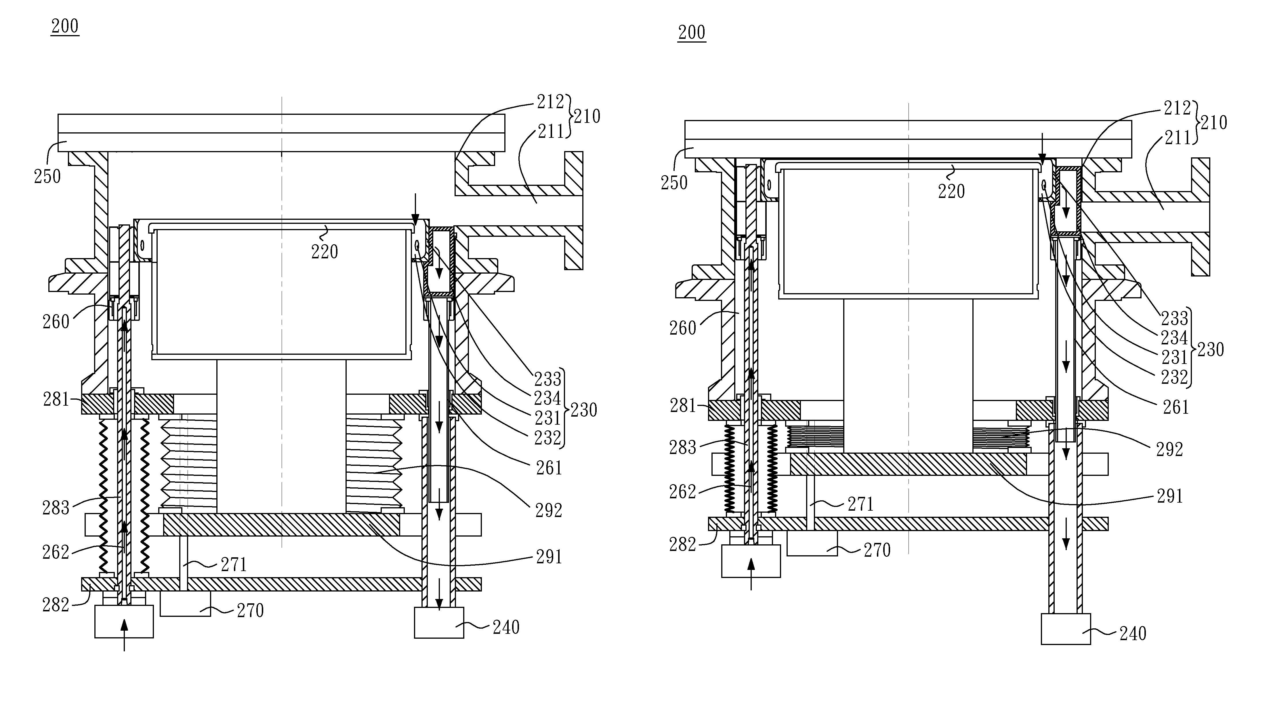
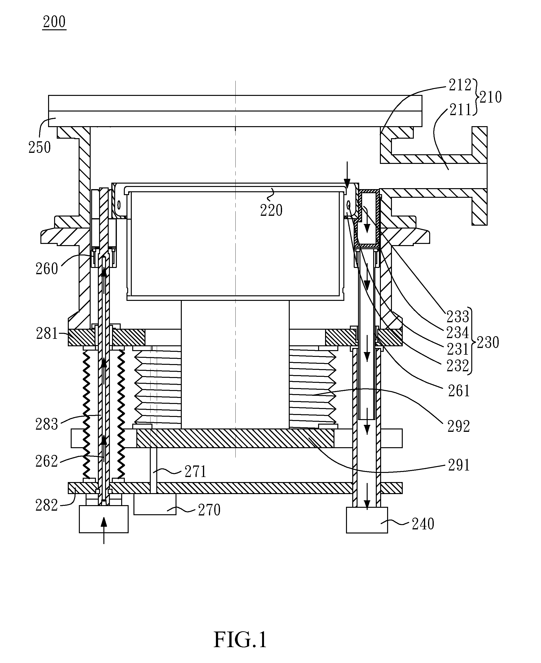
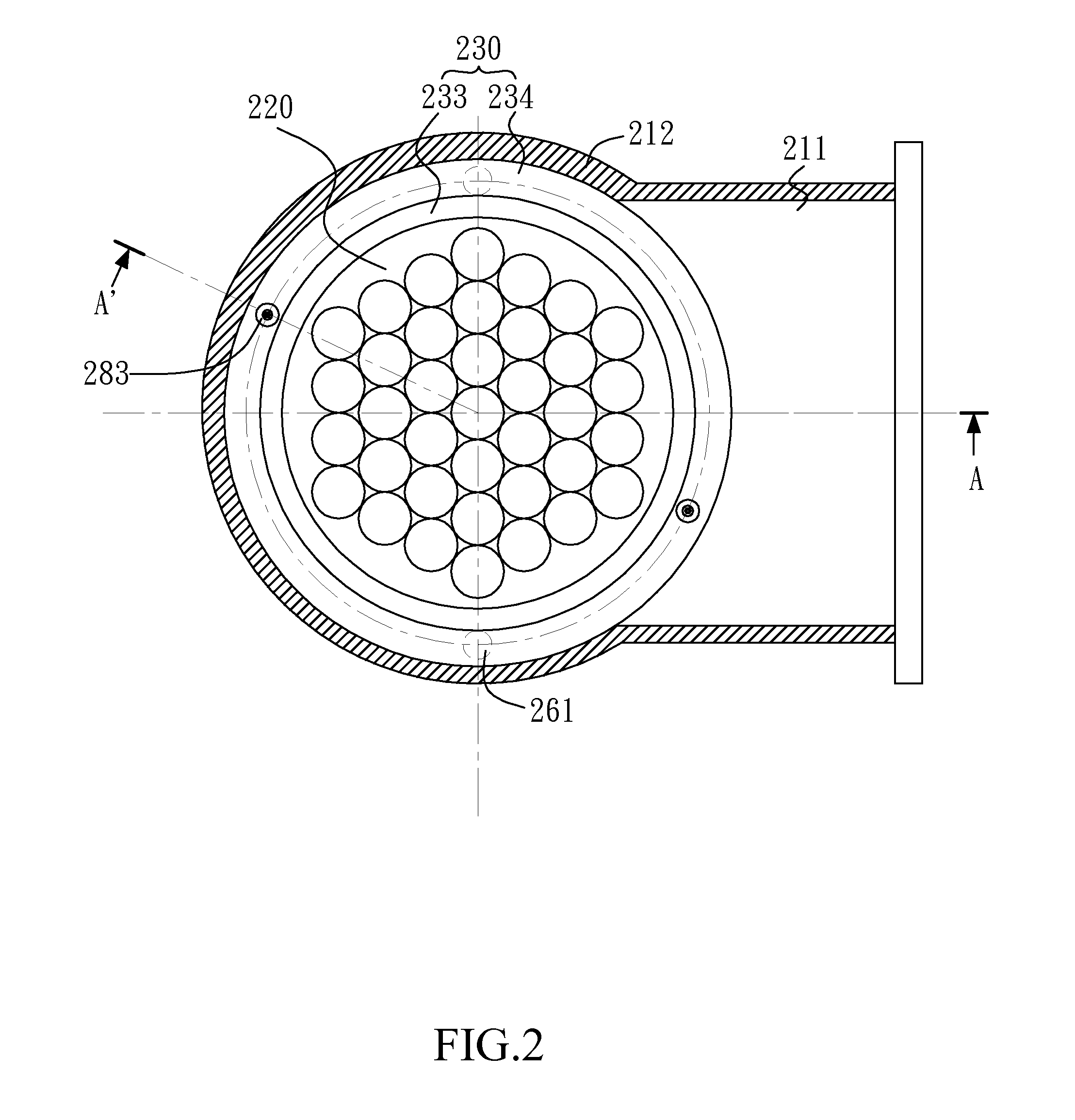
[0015]FIG. 1 shows a side view of the semiconductor equipment 200 in accordance with a preferred embodiment of the present invention. The semiconductor equipment 200 includes a reaction chamber 210, a wafer susceptor 220, a showerhead 250, and a liner device 230.

[0016]The wafer susceptor 220 is disposed within the reaction chamber 210, and the wafer susceptor 220 is capable of carrying at least one wafer. The showerhead 250 is disposed over the wafer susceptor 220. The reaction gases required by the semiconductor manufacturing process can be provided into the reac...


PUM

PropertyMeasurementUnit
temperatureaaaaaaaaaa
flexibleaaaaaaaaaa
lengthaaaaaaaaaa

Abstract

Semiconductor equipment is disclosed in this invention. The semiconductor equipment includes a reaction chamber, a wafer susceptor, and a liner device. The reaction chamber includes an opening and a circular inner wall. The wafer susceptor is capable of carrying at least one wafer. The liner device is disposed between the wafer susceptor and the circular inner wall of the reaction chamber. The liner device is capable of moving vertically between a first position and a second position. The liner device includes at least one venting opening, wherein the venting opening is connected with a venting device. Particles which are accumulated within the liner device can be removed by the venting device.

Description

CROSS-REFERENCE TO RELATED APPLICATIONS[0001]The entire contents of Taiwan Patent Application No. 100119661, filed on Jun. 3, 2011, from which this application claims priority, are incorporated herein by reference.BACKGROUND OF THE INVENTION[0002]1. Field of the Invention[0003]The present invention generally relates to semiconductor equipment, and more particularly to semiconductor equipment having cleaning function.[0004]2. Description of Related Art[0005]Semiconductor manufacturing equipment are commonly used in the production of semiconductor components. The semiconductor manufacturing equipment typically has a reaction chamber. The reaction gases required by the semiconductor manufacturing process can be provided into the reaction chamber by the showerhead of the reaction chamber. After several times of semiconductor manufacturing processes, particles or contaminants may be accumulated within the reaction chamber. Thus, process results and the process yields are affected by the ...

Claims


Application Information

Patent Timeline
Patent Type & Authority Patents(United States)
IPC IPC(8): H01J37/32H01L21/687C23C16/44H01L21/67
CPCH01J37/3288C23C16/4401C23C16/4411H01J37/32449H01J37/32513H01J37/32853H01J37/32871H01L21/67017H01L21/6719H01L21/68742
Inventor CHENG, JUI-SHENGHAN, TSUNG-HSUNHUANG, TSAN-HUA
Owner HERMES EPITEK
Why Eureka
Try Eureka