Integrated circuit having multiple threshold voltages

a technology of integrated circuits and threshold voltages, applied in the field of integrated circuits with multiple threshold voltages, can solve the problems of increased system cost, increased system footprint, and increased system complexity

Active Publication Date: 2016-06-07
GLOBALFOUNDRIES U S INC
View PDF17 Cites 287 Cited by
  • Summary
  • Abstract
  • Description
  • Claims
  • Application Information

AI Technical Summary

Problems solved by technology

A system using multiple discrete devices, each optimized for different functions, will result in greater system complexity, increased system footprint, and added system cost.

Method used


Image

  • Integrated circuit having multiple threshold voltages
  • Integrated circuit having multiple threshold voltages
  • Integrated circuit having multiple threshold voltages

Examples


Embodiment Construction

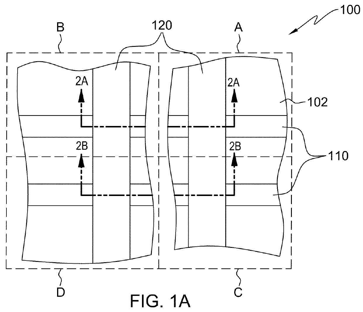
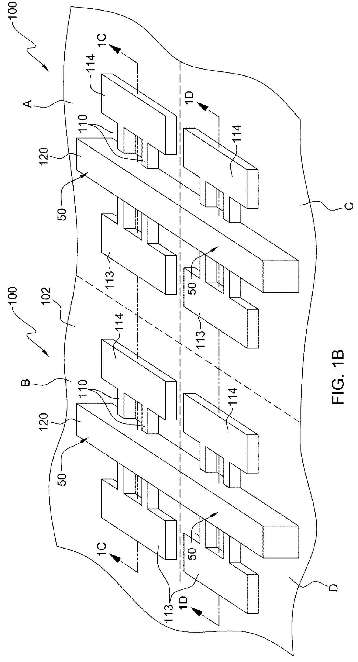
[0031]In one aspect there is set forth herein a semiconductor device having a first plurality of field effect transistors and a second plurality of field effect transistors, wherein field effect transistors of the first plurality of field effect transistors each have a first gate stack and wherein field effect transistors of the second plurality of field effect transistors each have a second gate stack, the second gate stack being different from the first gate stack by having a conductive layer common to the first gate stack and the second gate stack that includes a first thickness at the first gate stack and a second thickness at the second gate stack.

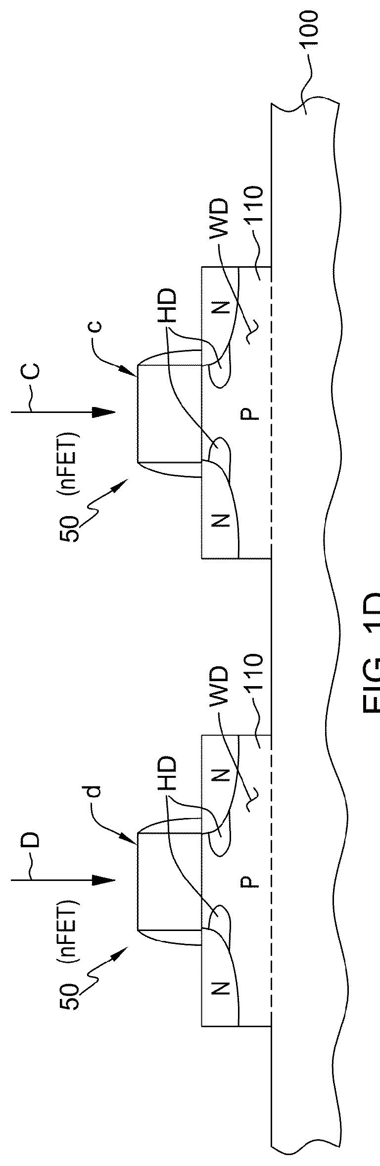
[0032]In one aspect there is set forth herein a semiconductor device having a first field effect transistor formed in a substrate structure, and a second field effect transistor formed in the substrate structure. The first field effect transistor can include a first substrate structure doping, a first gate stack, and a first threshold...


PUM


Abstract

In one aspect there is set forth herein an integrated circuit having a first plurality of field effect transistors and a second plurality of field effect transistor, wherein field effect transistors of the first plurality of field effect transistors each have a first gate stack and wherein field effect transistors of the second plurality of field effect transistors each have a second gate stack, the second gate stack being different from the first gate stack by having a metal layer common to the first gate stack and the second gate stack that includes a first thickness at the first gate stack and a second thickness at the second gate stack.

Description

FIELD OF THE INVENTION[0001]The present invention relates to semiconductor devices and methods of manufacturing semiconductor devices, and more particularly, to an integrated circuit having multiple threshold voltages.BACKGROUND OF THE INVENTION[0002]Different semiconductor devices may be fabricated to have one or more different device characteristics, such as switching speed, leakage power consumption, etc. Multiple different designs may each provide optimization of one or more of these characteristics for devices intended to perform specific functions. For instance, one design may increase switching speed for devices providing computational logic functions, and another design may decrease power consumption for devices providing memory storage functions. A system using multiple discrete devices, each optimized for different functions, will result in greater system complexity, increased system footprint, and added system cost.BRIEF SUMMARY[0003]In one aspect there is set forth herei...

Claims


Application Information

Patent Timeline
Patent Type & Authority Patents(United States)
IPC IPC(8): H01L21/8238H01L29/49H01L21/28H01L21/8234H01L27/088H01L27/092
CPCH01L21/823842H01L21/28088H01L21/82345H01L21/823431H01L27/088H01L27/0886H01L27/092H01L27/0922H01L27/0924H01L29/4966H01L29/66545
Inventor LEE, BONGKILIU, JIN PINGJOSHI, MANOJELLER, MANFREDPAL, ROHITCARTER, RICHARD J.SAMAVEDAM, SRIKANTH BALAJI
Owner GLOBALFOUNDRIES U S INC
Why Eureka
Try Eureka