Display device and method for producing a display device

a display device and display device technology, applied in the direction of semiconductor devices, basic electric elements, electrical apparatus, etc., can solve the problem of ever higher current through the pixel, and achieve the effect of high refresh rate, efficient and simple production of display devices

Active Publication Date: 2016-06-07
OSRAM OLED
View PDF20 Cites 67 Cited by
  • Summary
  • Abstract
  • Description
  • Claims
  • Application Information

AI Technical Summary

Benefits of technology

[0004]Embodiments of the invention provide a display device that allows images to be generated with high resolution and a high refresh rate. In addition, a method is provided with which a display device can be efficiently and simply produced.
[0008]In a preferred embodiment a semiconductor layer sequence growth substrate is removed completely or at least in places or is thinned throughout or at least in places. The carrier may stabilize the semiconductor layer sequence mechanically, which means that the growth substrate is no longer needed for this purpose. The display device is preferably completely free of the growth substrate. The risk of optical crosstalk between adjacent pixels when the display device is in operation can thus be reduced. In contrast thereto, however, it may also be sufficient for the growth substrate merely to be thinned to a given residual thickness.
[0011]One of the connection layers may form a common electrical contact for the pixels, for example, the first connection layer may form a common electrical contact for the first semiconductor layer and the second semiconductor layer of the pixels may be connected electrically conductively by means of the second connection layer in each case with one of the switches, or vice versa. With a common electrical contact for a plurality of pixels, in particular for all the pixels, the total number of contacts required for the pixels may be reduced.
[0015]Alternatively, the trench may also be formed only in the first semiconductor layer, i.e., the trench does not divide the active region. Such a trench may improve optical separation between the pixels, without the active region being divided.

Problems solved by technology

In this method the pixels can only be driven one after the other, which results in ever higher currents through the pixel in the case of an increasing number of pixels for flicker-free overall display device brightness.

Method used


Image

  • Display device and method for producing a display device
  • Display device and method for producing a display device
  • Display device and method for producing a display device

Examples


Embodiment Construction

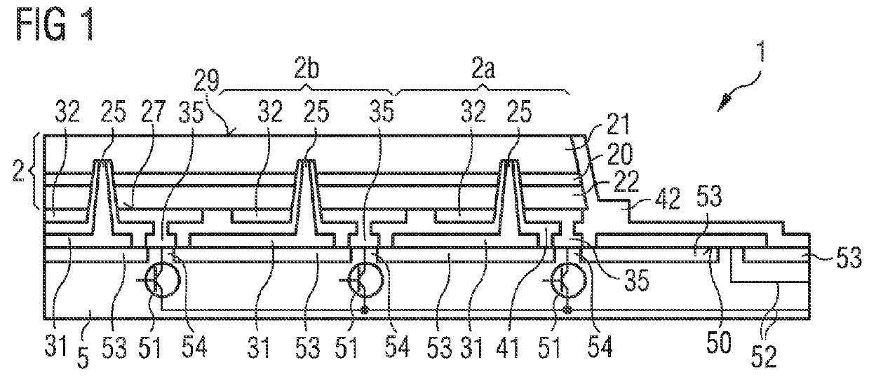
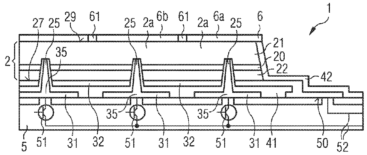
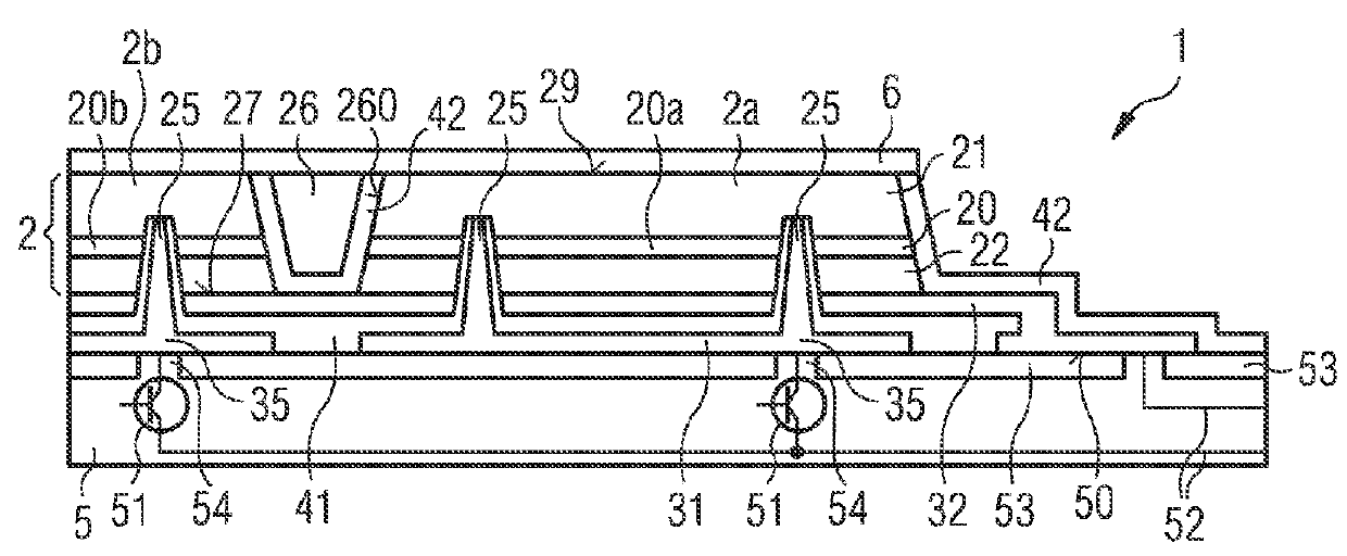
[0036]FIG. 1 is a schematic sectional view of a first exemplary embodiment of a display device 1. The display device comprises a plurality of pixels, which are arranged next to one another, in particular in the manner of a matrix. To simplify the illustration, a portion of the display device with a first pixel 2a and a second pixel 2b is shown in the figure.

[0037]The display device 1 comprises a semiconductor layer sequence 2. The semiconductor layer sequence comprises an active region 20 provided for generating radiation, which region extends vertically between a major face 27 and a radiation exit face 29. The active region is arranged between a first semiconductor layer 21 of a first conduction type and a second semiconductor layer 22 of a second conduction type different from the first conduction type. For example, the first semiconductor layer may be n-conductive and the second semiconductor layer p-conductive or vice versa. In the semiconductor layer sequence 2 a plurality of r...


PUM


Abstract

A display device with a semiconductor layer sequence includes an active region provided for generating radiation and a plurality of pixels. The display device also includes a carrier. The active region is arranged between a first semiconductor layer and a second semiconductor layer. The semiconductor layer sequence includes at least one recess, which extends from a major face of the semiconductor layer sequence facing the carrier through the active region into the first semiconductor layer and is provided for electrical contacting of the first semiconductor layer. The carrier includes a plurality of switches, which are each provided for controlling at least one pixel.

Description

[0001]This patent application is a national phase filing under section 371 of PCT / EP2012 / 075080, filed Dec. 11, 2012, which claims the priority of German patent application 10 2011 056 888.3, filed Dec. 11, 2011, each of which is incorporated herein by reference in its entirety.TECHNICAL FIELD[0002]A display device and a method for producing a display device are provided.BACKGROUND[0003]LED display devices with a small number of pixels may be driven by the multiplexing method, in which for each pixel one contact per row and one contact per column is passed out and supplied to a controller. In this method the pixels can only be driven one after the other, which results in ever higher currents through the pixel in the case of an increasing number of pixels for flicker-free overall display device brightness.SUMMARY OF THE INVENTION[0004]Embodiments of the invention provide a display device that allows images to be generated with high resolution and a high refresh rate. In addition, a m...

Claims


Application Information

Patent Timeline
Patent Type & Authority Patents(United States)
IPC IPC(8): H01L33/00H01L27/15H01L33/50H01L33/38
CPCH01L27/156H01L27/15H01L33/005H01L33/50H01L33/382H01L27/124H01L27/1259H01L33/20H01L33/505H01L33/62H01L2933/0066
Inventor VON MALM, NORWIN
Owner OSRAM OLED
Why Eureka
Try Eureka