Communication terminal device

a terminal device and communication terminal technology, applied in loop antennas with ferromagnetic cores, instruments, sensing by electromagnetic radiation, etc., can solve the problems of reducing the radiation characteristics of antennas by power feeding coils and planar conductors, increasing thickness and size, and high cost of magnetic body sheets, so as to ensure antenna characteristics, reduce the effect of induced current generation in rear metal bodies and sufficient communication distan

Active Publication Date: 2016-11-22
MURATA MFG CO LTD
View PDF10 Cites 1 Cited by
  • Summary
  • Abstract
  • Description
  • Claims
  • Application Information

AI Technical Summary

Benefits of technology

[0008]Preferred embodiments of the present invention provide a communication terminal device that significantly reduces or prevents induced current generated in a rear metal body and ensures antenna characteristics without increasing a size of a magnetic body sheet that provides magnetic shielding.
[0010]According to various preferred embodiments of the present invention, induced current that is generated in a rear metal body is significantly reduced or prevented, and antenna characteristics are ensured without providing a thick and large magnetic body sheet to provide magnetic shielding. Therefore, the communication terminal device ensures a sufficient communication distance while being reduced in size and increased in density.

Problems solved by technology

This results in the lowering of antenna radiation characteristics by the power feeding coil and the planar conductor in some cases.
However, the magnetic body sheet is expensive, and an increase thereof in thickness and size leads increase in cost.

Method used


Image

  • Communication terminal device
  • Communication terminal device
  • Communication terminal device

Examples


first preferred embodiment

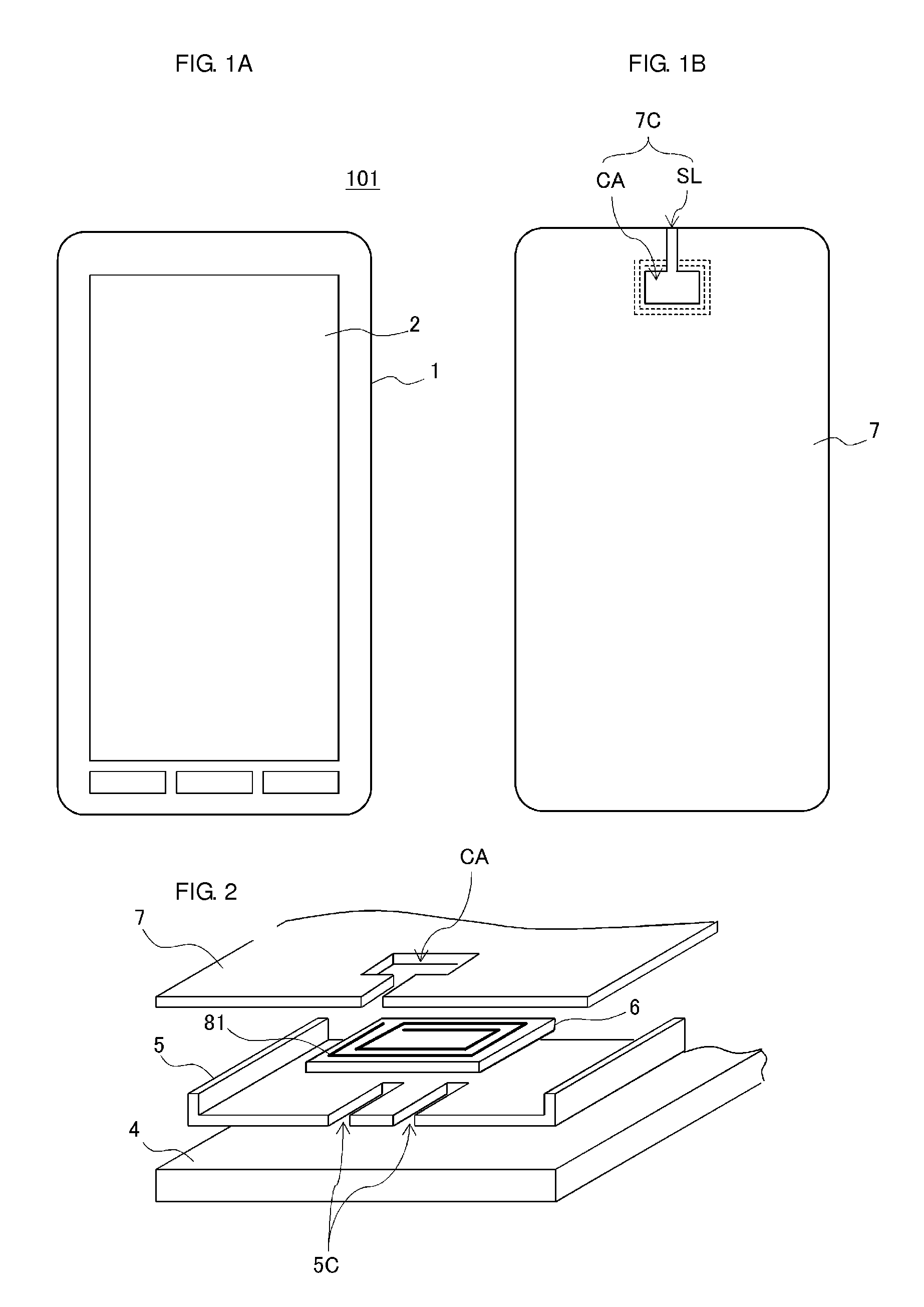
[0029]FIG. 1 includes outer appearance views illustrating a communication terminal device 101 according to a first preferred embodiment of the present invention, and FIG. 1A is a front view and FIG. 1B is a rear view. A front housing 1 is observed at the front side of the communication terminal device 101 and the front surface of a display / touch panel 2 is exposed. A planar radiation conductor 7 as a rear surface cover is provided on the rear surface of the communication terminal device 101 as an outer surface of the device. The planar radiation conductor 7 is an aluminum molded product, for example. A cutout portion 7C including a conductor opening CA and a slit portion SL is provided in the planar radiation conductor 7. The conductor opening CA defines and serves as a lens opening of a camera module, for example, in some cases, but it is not illustrated in FIG. 1B.

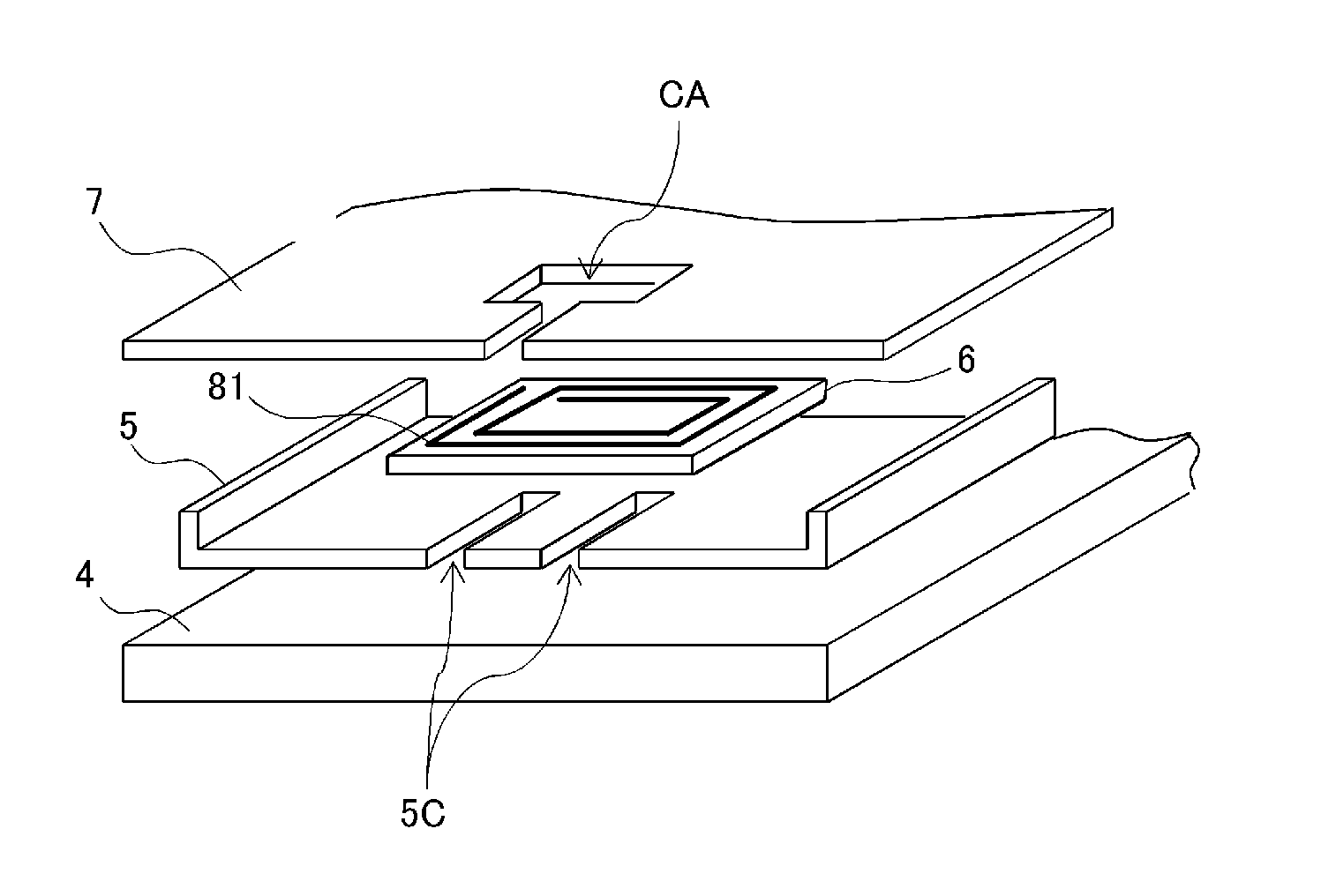
[0030]FIG. 2 is an exploded perspective view of a main portion of the communication terminal device 101. A rear metal ...

second preferred embodiment

[0063]FIG. 8 is an exploded perspective view of a main portion of a communication terminal device according to a second preferred embodiment of the present invention. The rear metal body 5 as a shield plate and the printed wiring board 4 are accommodated between the front housing and the planar radiation conductor (rear surface cover) 7. Further, the power feeding coil 81 and the magnetic body sheet 6 are arranged between the planar radiation conductor 7 and the rear metal body 5.

[0064]Various circuits are provided on the printed wiring board 4. A power feeding circuit that is connected to the power feeding coil 81 is also provided on the printed wiring board 4. The rear metal body 5 is a molded product including a metal plate, for example. The punched portions 5C are provided on the rear metal body 5.

[0065]An integrated circuit IC 3 is mounted on the printed wiring board 4. The rear metal body 5 covers a range of the printed wiring board 4, which includes the IC 3 and the like. Oth...

third preferred embodiment

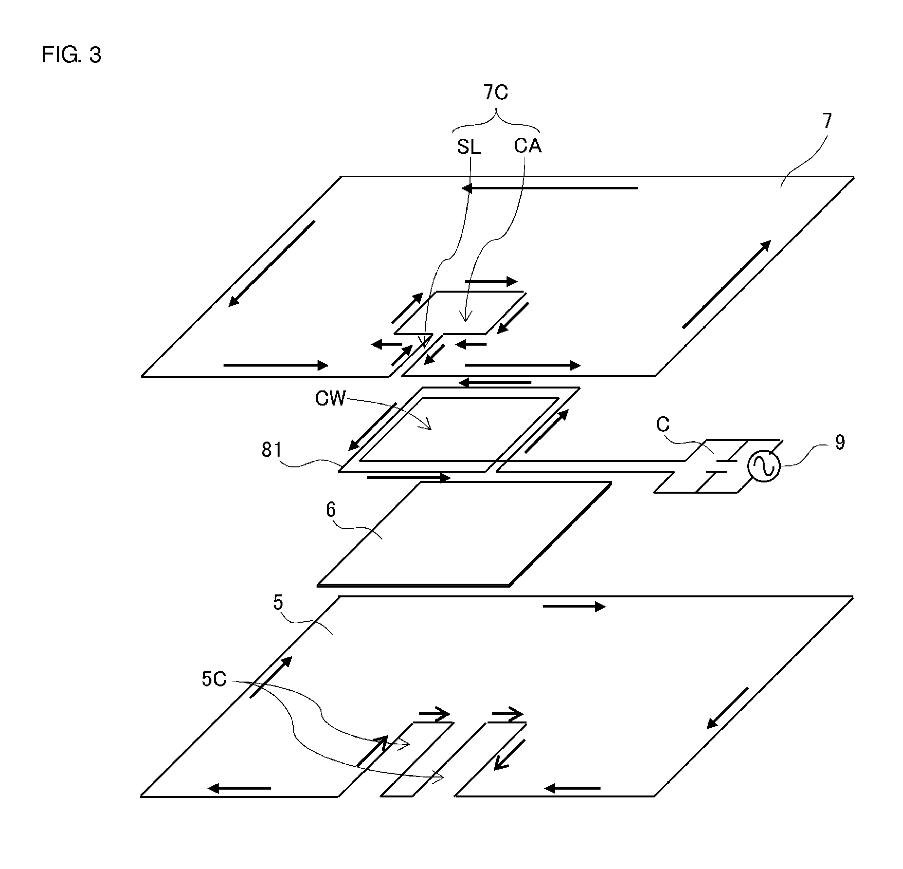
[0068]FIG. 9 is a schematic exploded perspective view of a main part of a communication terminal device according to a third preferred embodiment of the present invention, and is a view illustrating current flowing through the power feeding coil 81, the planar radiation conductor 7, and the rear metal body 5. The communication terminal device is different from the communication terminal device as described in the first preferred embodiment in a shape of a cutout portion of the planar radiation conductor 7.

[0069]In the present preferred embodiment, a cutout portion including the conductor opening CA having a circular or substantially circular shape and the slit portion SL is provided on the planar radiation conductor 7. Other configurations preferably are the same as those in the first preferred embodiment.

[0070]FIGS. 10A, 10B, 10C, and 10D are views illustrating a positional relationship among the above-mentioned individual members when viewed in a plan view. FIG. 10A is a plan view...


PUM

PropertyMeasurementUnit
inductanceaaaaaaaaaa
lengthaaaaaaaaaa

Abstract

A communication terminal device includes a power feeding coil connected to a power feeding circuit, a planar radiation conductor arranged in the vicinity of the power feeding coil and including a cutout portion overlapping with a coil opening of the power feeding coil when viewed in a plan view, and a rear metal body arranged at a side opposite to the planar radiation conductor with respect to the power feeding coil and in the vicinity of the planar radiation conductor, wherein a punched portion which does not overlap with at least a portion of the power feeding coil when viewed in a plan view and has a shape different from a shape of the cutout portion on the planar radiation conductor is provided on the rear metal body.

Description

BACKGROUND OF THE INVENTION[0001]1. Field of the Invention[0002]The present invention relates to a communication terminal device that is preferably used for a radio-frequency identification device (RFID) system and a near field communication system.[0003]2. Description of the Related Art[0004]In an RFID system in a high frequency (HF) range and a near field communication (NFC) system, an antenna for communication is mounted on each communication terminal device such as a cellular phone terminal in order to perform communication between the communication terminal device and a reader / writer or perform communication between the communication terminal devices. Japanese Patent No. 4687832 discloses an antenna that is provided on a communication terminal device as described above.[0005]As disclosed in Japanese Patent No. 4687832, an opening and a slit are provided on a planar conductor to which a power feeding coil comes close such that current induced by a magnetic field generated in the...

Claims


Application Information

Patent Timeline
Patent Type & Authority Patents(United States)
IPC IPC(8): H01Q1/24H01F27/36H01Q1/52H01F38/14H01Q7/00G06K7/10H01Q1/22
CPCH01Q1/243G06K7/10336H01F27/367H01F38/14H01Q1/2216H01Q1/52H01Q7/00H01F27/36H01F27/361H01Q7/06
Inventor MURAYAMA, HIROMINAKANO, SHINICHI
Owner MURATA MFG CO LTD
Why Eureka
Try Eureka