

Lead-free solder ball
a solder ball and lead-free technology, applied in the direction of soldering apparatus, semiconductor/solid-state device details, manufacturing tools, etc., can solve the problems of not only a great deal of effort, but also the inability to supply solder from the exterior to the electrode, so as to minimize and reduce the occurrence of failur
- Summary
- Abstract
- Description
- Claims
- Application Information
AI Technical Summary
Benefits of technology
Problems solved by technology
Method used
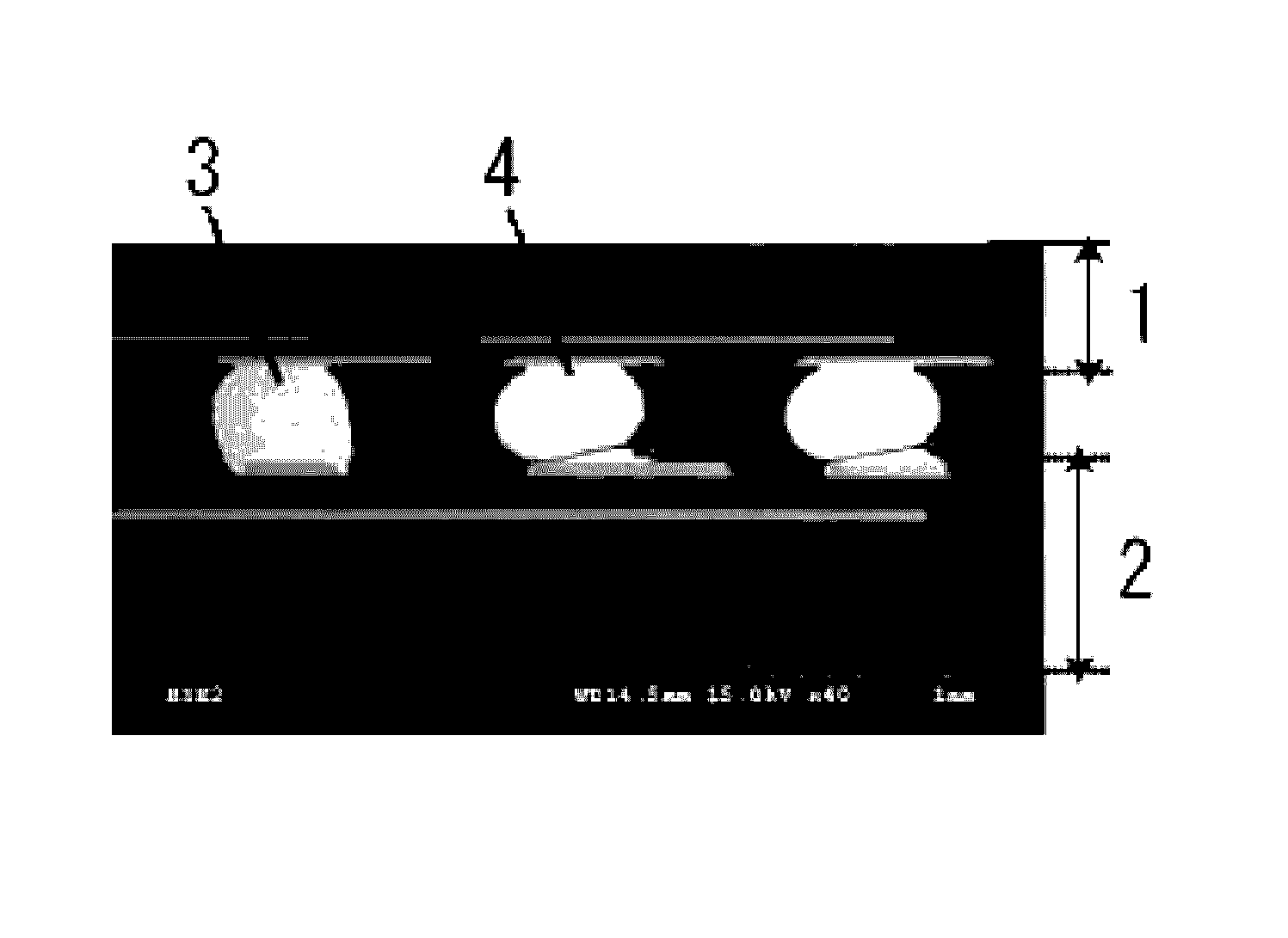
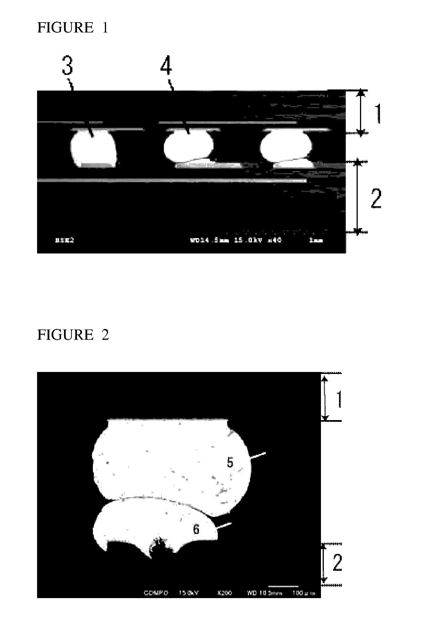
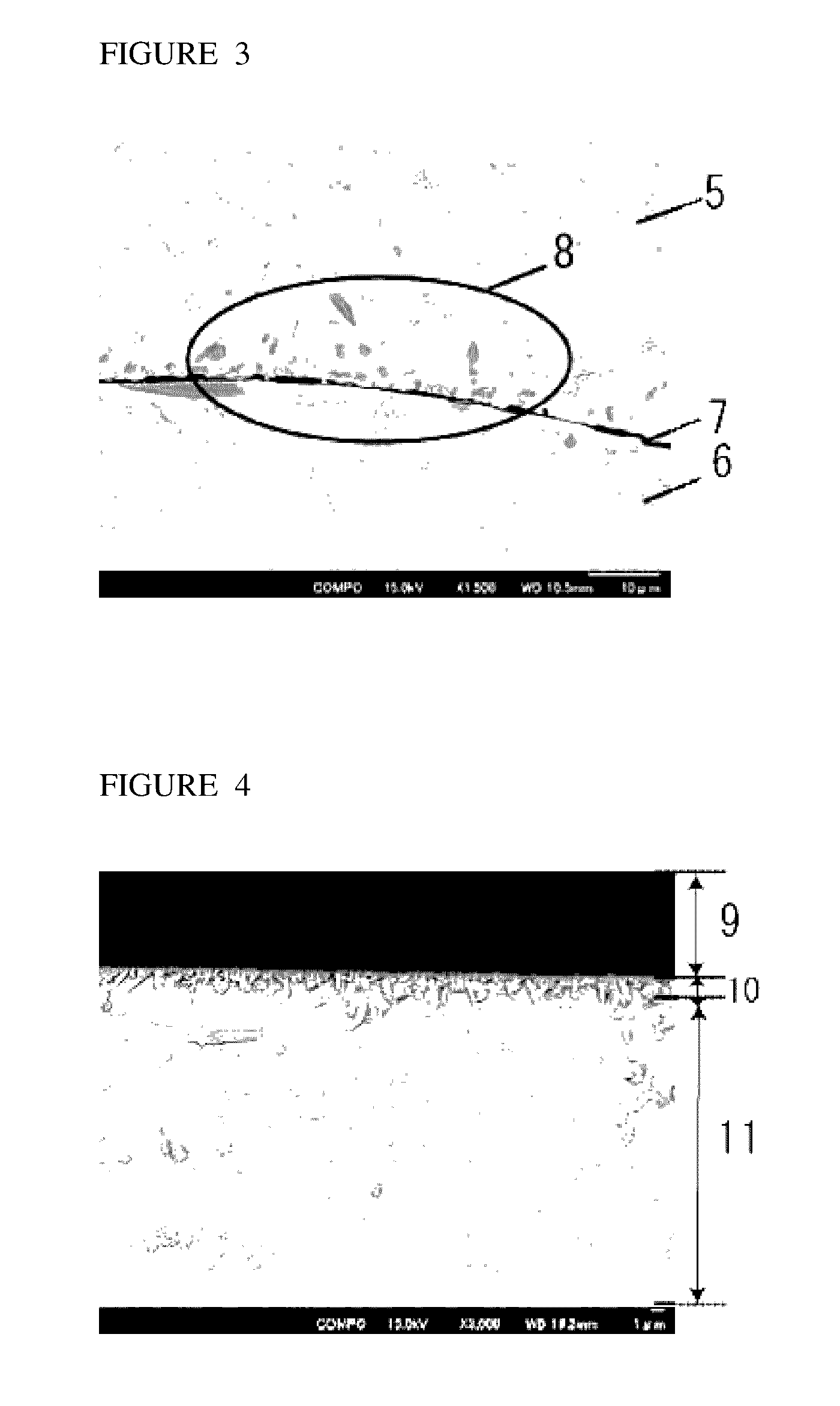
Image

Examples
examples
[0038]Solder alloys having the composition shown in the following table were prepared, and solder balls having a diameter of 0.3 mm were prepared by the droplet spraying method. These solder balls were used to fabricate CSP substrates by the following procedure.
[0039]
TABLE 1Solder compositionOccurrenceResistance to drop impacts(mass %)of fusionSpreading(number of drops)SnAgCuNidefects (%)(mm2)Ni / AuNi / Pd / AuCu-OSPCommentsExample1Rem0.50.70.051.20.768072952Rem10.70.054.90.828346503Rem10.70.072.50.806279584Rem10.70.082.90.8683771235Rem10.750.071.80.859881946Rem10.80.054.30.813459467Rem10.80.074.00.813758678Rem10.80.082.20.796574899Rem1.10.80.073.70.9143534910Rem1.10.80.082.80.88486668Comparative1Rem00.71.60.55592Example2Rem0.30.70.050.50.58786547Pat. Doc. 33Rem10.51.80.87158544Rem10.50.023.20.854—335Rem10.50.050.50.881—506Rem10.70.020.90.9010—367Rem10.70.110.60.7412—18Rem10.80.024.60.87522159Rem10.80.112.50.74816110Rem118.60.8611111Rem110.0515.70.81111Pat. Doc. 412Rem1.20.50.024.40.8231...
PUM
| Property | Measurement | Unit |
|---|---|---|
| mass % | aaaaa | aaaaa |
| mass % | aaaaa | aaaaa |
| impurities | aaaaa | aaaaa |
Abstract
Description
Claims
Application Information