Check patentability & draft patents in minutes with Patsnap Eureka AI!

Charged particle beam device and arithmetic device

a charge particle and beam technology, applied in the direction of electrical discharge tubes, instruments, electrical apparatus, etc., can solve the problems of complex adjustment operations, difficult to take a measure, and inability to independently detect aberrations

Active Publication Date: 2016-12-27
HITACHI HIGH-TECH CORP
View PDF9 Cites 0 Cited by
  • Summary
  • Abstract
  • Description
  • Claims
  • Application Information

AI Technical Summary

Benefits of technology

[0019]According to the present invention, it is possible to, even when the relationship between the field intensity of multiple poles of an aberration corrector and a parasitic aberration adjustment amount changes nonlinearly or changes with time, correct parasitic aberrations by suppressing the influence of the change. Other problems, configurations, and advantages will become apparent from the following

Problems solved by technology

However, as the aberration corrector needs a large number of power supplies for the multiple poles, complicated adjustment operations are required.
However, a field that is necessary to correct each aberration is not independent of each other.
However, as an aberration occurs due to a positional deviation of each pole of the multipole lens in the aberration corrector, variations in the magnetic properties of polar materials, and the like, there may be cases where a distribution of the generated field would deviate from the ideal field distribution of the multiple poles even when the electric field or magnetic field of the multipole lens is controlled.
Therefore, it would be difficult to take a measure by predicting a deviation that may occur through simulation or the like before producing an aberration corrector.
This is because, if a charged particle beam does not reach the surface of the sample due to a significant axis deviation originating from parasitic aberrations and acquisition of an image has thus failed, or if a big out-of-focus has occurred and the image quality has thus deteriorated to such an extent that the sample cannot be identified as a result of changing the field of the multiple poles, it would be impossible to compute the magnitude of an aberration from the image and execute a continuous aberration correction sequence.

Method used


Image

  • Charged particle beam device and arithmetic device
  • Charged particle beam device and arithmetic device
  • Charged particle beam device and arithmetic device

Examples


embodiment 1

System Configuration

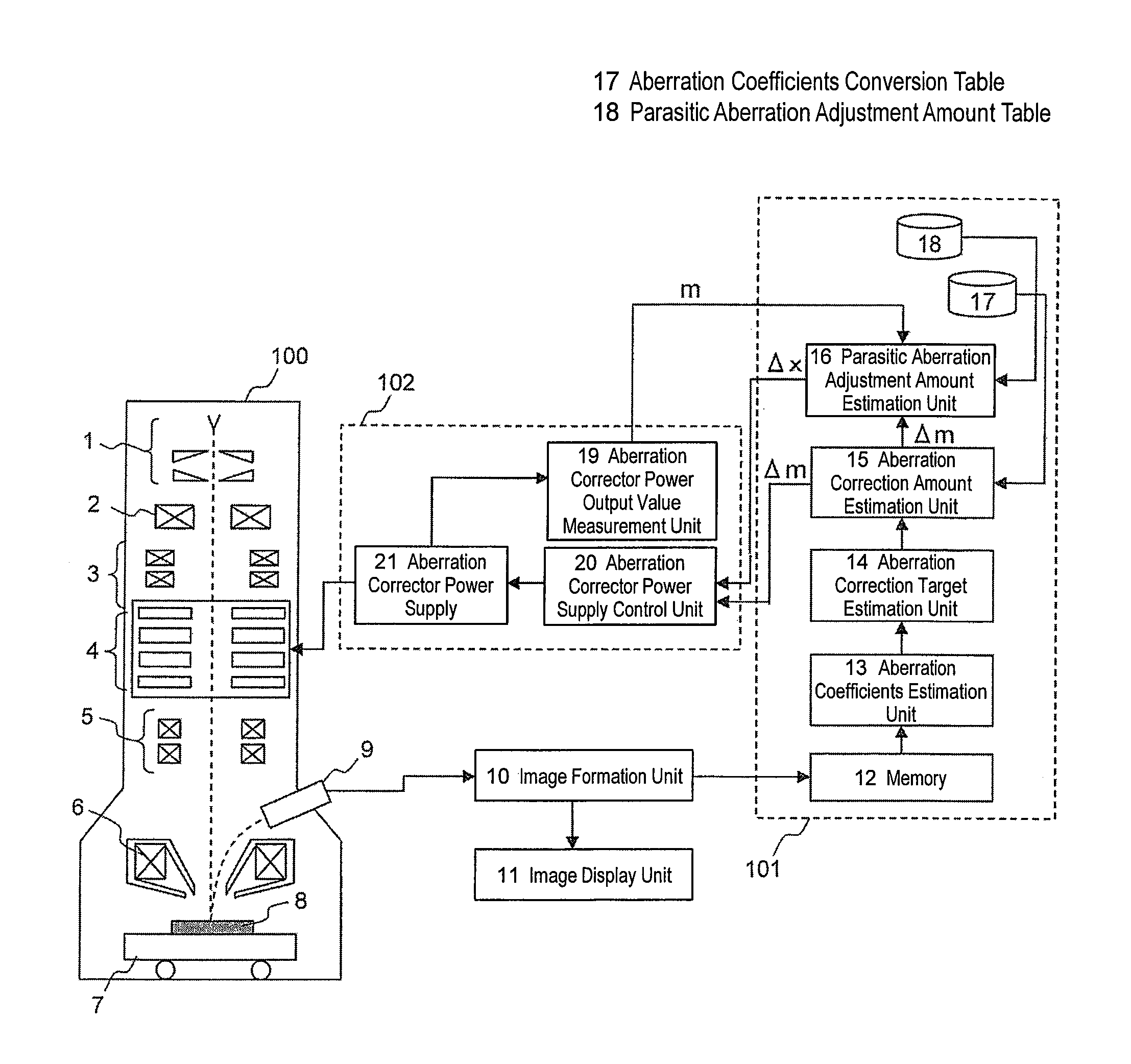
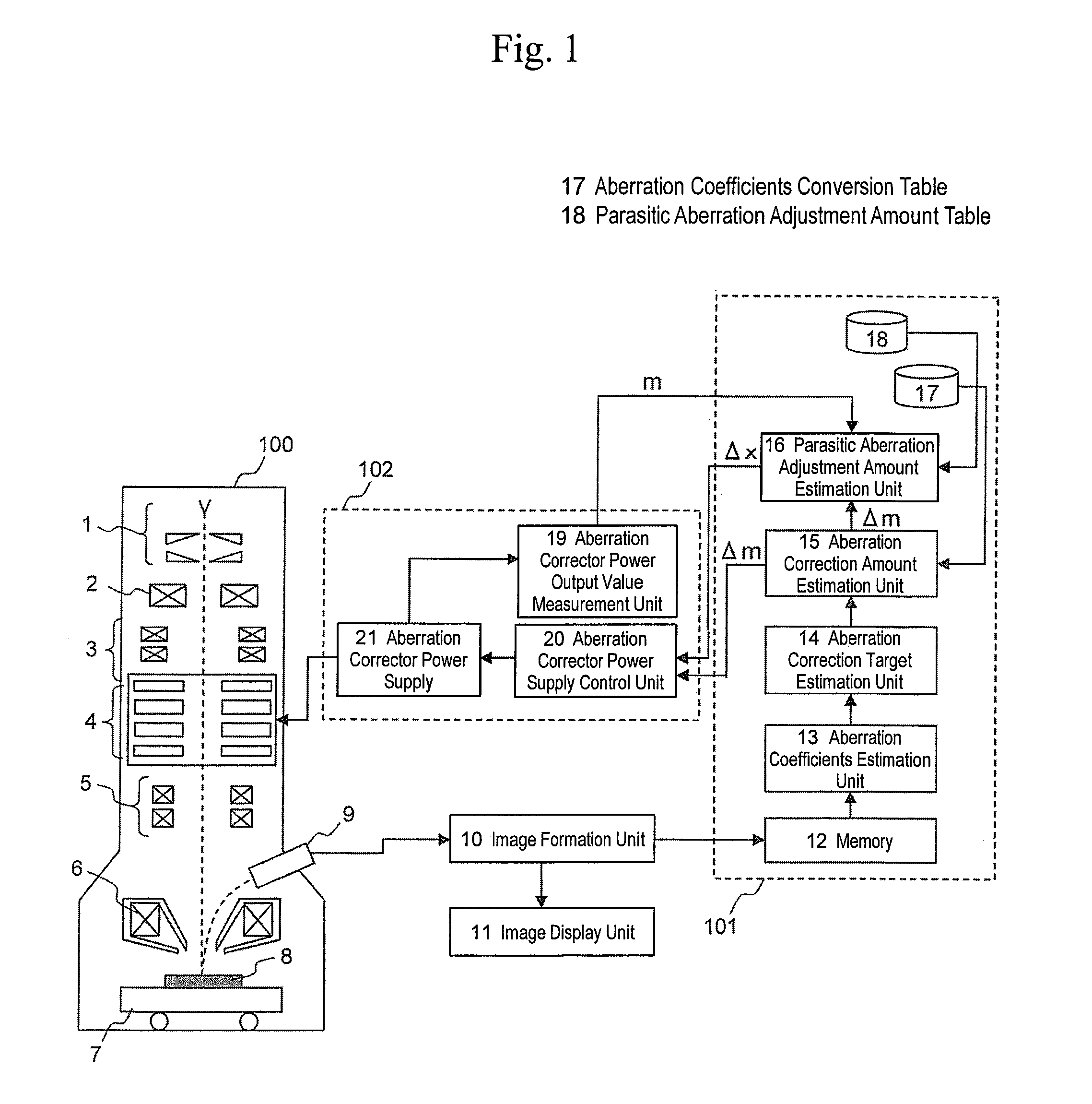
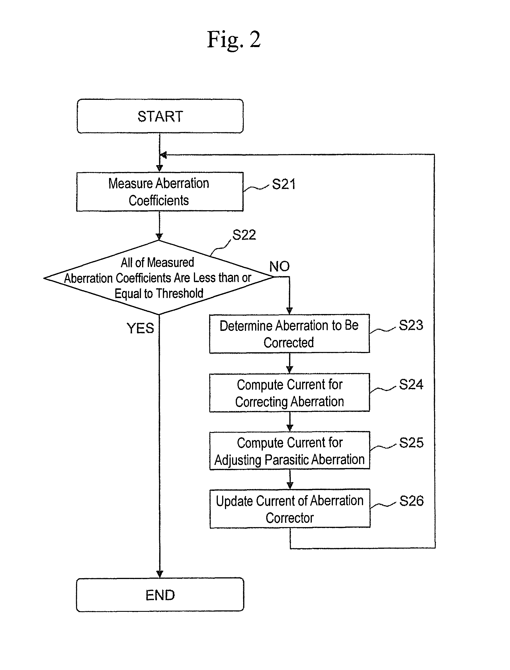
[0032]FIG. 1 shows the schematic configuration of a SEM system that has an aberration corrector mounted thereon. This embodiment will describe a SEM that has mounted thereon a quadrupole to octupole-electromagnetic-field-superimposed aberration corrector, and a control system therefor.

[0033]An electron beam (which is indicated by the dotted line in FIG. 1) emitted from an electron gun 1 in a SEM column 100 enters an aberration corrector 4 after passing through a condenser lens 2 and a two-stage deflection coil 3. An electron beam that has passed through the aberration corrector 4 further passes through a scan coil 5 and an objective lens 6, and then scans the surface of a sample 8 mounted on a sample stage 7. Secondary charged particles, such as secondary electrons or reflected electrons, are emitted from a point of the sample 8 irradiated with the electron beam. The secondary charged particles are detected by a detector 9, and the detection result is output to a...

embodiment 2

System Configuration

[0061]FIG. 6 shows the schematic configuration of a SEM system in accordance with Embodiment 2. In FIG. 6, portions corresponding to those in FIG. 1 are denoted by the same reference numerals. The SEM system in accordance with this embodiment also has mounted thereon a quadrupole to octopole electromagnetic field superimposed aberration corrector. As described below, the SEM system in accordance with this embodiment records a measurement history of the present value (i.e., power output value) of the multipole control amount provided to each of the multiple poles of the aberration corrector 4 and a measurement history of the aberration amount, and computes an optimal parasitic aberration adjustment amount at each point in time with reference to the measurement history.

[0062]Hereinafter, only points that differ from those in Embodiment 1 will be described. First, in this embodiment, the aberration coefficients estimation unit 13 has an aberration coefficients measu...


PUM


Abstract

It is possible to determine an optimal parasitic aberration adjustment amount even when the relationship of the parasitic aberration adjustment amount with respect to the field intensity of multiple poles changes nonlinearly. To this end, in the present invention, an aberration correction amount is computed by measuring an aberration coefficient of an optical unit of a charged particle beam device, and at the same time, the present value of a power supply control value applied to an aberration corrector is measured. Then, the parasitic aberration adjustment amount for suppressing the amount of a parasitic aberration generated in the aberration corrector is computed on the basis of the aberration correction amount and the present value of the power supply control value.

Description

TECHNICAL FIELD[0001]The present invention relates to a technique of automatically adjusting parasitic aberrations in a charged particle beam device having an automatic aberration corrector.BACKGROUND ART[0002]A scanning electron microscope (SEM), a focused ion beam (FIB) processing device, or a device that uses other types of converged charged particle beams (i.e., probe beams) observes an image of a sample and processes the sample by scanning the surface of the sample with a probe. The resolution and the processing accuracy of such charged particle beam device are determined by the size of the probe cross-section (i.e., probe diameter). In principle, the smaller the probe diameter, the higher the resolution and processing accuracy that can be achieved.[0003]In recent years, aberration correctors for charged particle beam devices have been developed and put into practical use. For an aberration corrector, multiple stages of multipole lenses having magnetic poles or electrodes are u...

Claims


Application Information

Patent Timeline
Patent Type & Authority Patents(United States)
IPC IPC(8): H01J37/28H01J37/153G01Q40/00
CPCH01J37/28G01Q40/00H01J37/153H01J2237/1534H01J2237/28H01J2237/2809
Inventor URANO, KOTOKONAKANO, TOMONORIOSE, YOICHI
Owner HITACHI HIGH-TECH CORP
Features
  • R&D
  • Intellectual Property
  • Life Sciences
  • Materials
  • Tech Scout
  • Unparalleled Data Quality
  • Higher Quality Content
  • 60% Fewer Hallucinations
Learn More