Substrate bias circuit and method for biasing a substrate

a substrate and bias circuit technology, applied in the field of circuits, can solve problems such as unsatisfactory current path, excessive current consumption, and latch-up of the integrated circui

Active Publication Date: 2017-02-28
NXP USA INC
View PDF17 Cites 62 Cited by
  • Summary
  • Abstract
  • Description
  • Claims
  • Application Information

AI Technical Summary

Problems solved by technology

However, during power-up of an integrated circuit configured to provide reverse back biasing, if the well bias is applied after the power supply voltage is applied, a condition may exist that creates an undesirable current path through series-connected N-channel and P-channel transistors.
The condition may lead to excessive current consumption, and in high temperature cases, may result in latch-up of the integrated circuit.

Method used


Image

  • Substrate bias circuit and method for biasing a substrate
  • Substrate bias circuit and method for biasing a substrate
  • Substrate bias circuit and method for biasing a substrate

Examples


Embodiment Construction

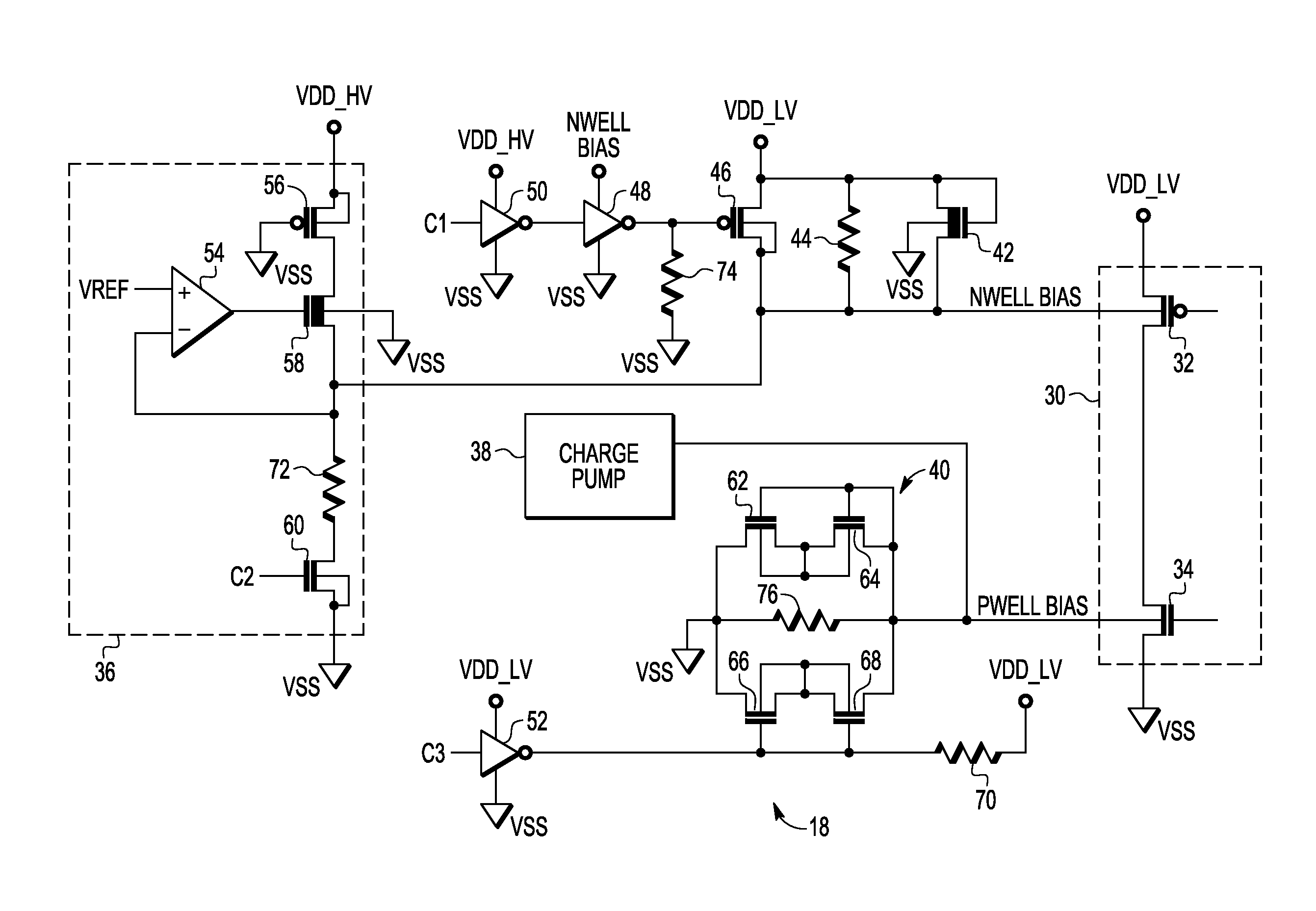
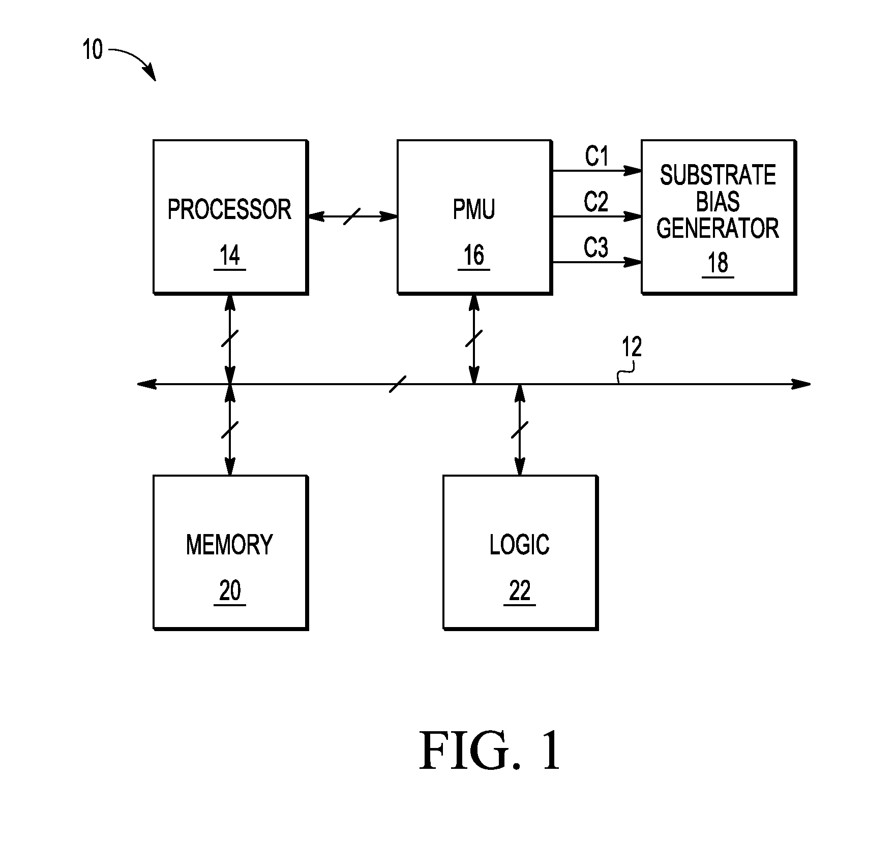
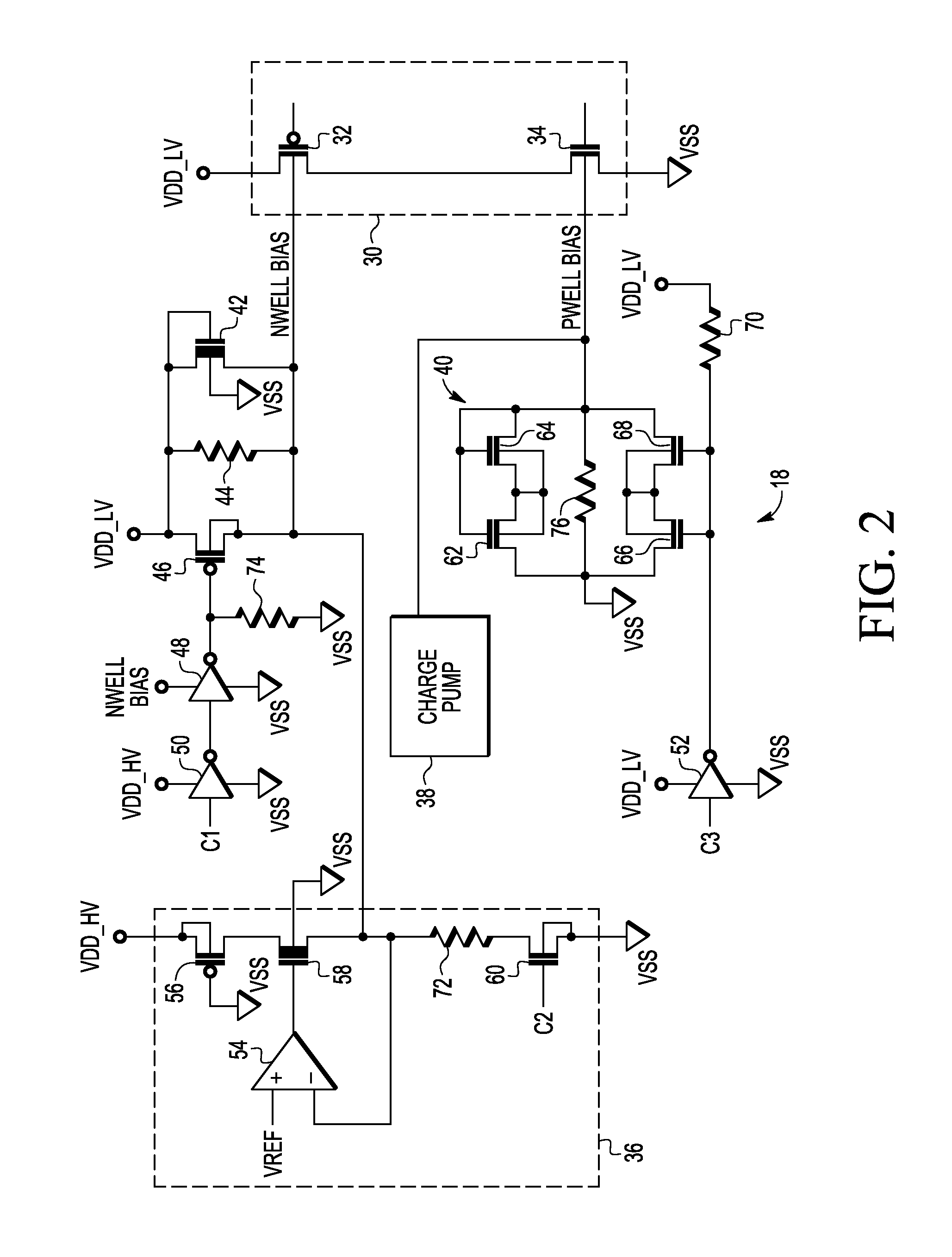
[0009]Generally, there is provided, a substrate bias circuit that provides reverse back biasing for transistors of an integrated circuit. In one embodiment, the integrated circuit includes an N-well for P-channel transistors and a P-well for N-channel transistors. Instead of coupling the N-well and P-well terminals to the power supply and ground, respectively, the N-well and P-well terminals are reverse back biased by the substrate bias circuit. The substrate bias circuit provides reverse back biasing by providing a voltage greater than the power supply voltage to the N-well and a voltage lower than ground to the P-well. The substrate bias circuit includes a depletion N-channel transistor that is diode-connected between a power supply voltage terminal and the substrate, or body, terminals of the P-channel transistors in the N-well. The substrate bias circuit also includes back-to-back diode-connected transistors connected between ground and the P-well substrate terminals of the N-ch...


PUM


Abstract

A substrate bias circuit and method for biasing a substrate are provided. A substrate bias circuit includes a first voltage source, a second voltage source, a diode coupled between the first voltage source and the second voltage source, and a plurality of transistors, each transistor in the plurality of transistors having a substrate terminal. In one example, the first voltage source supplies, via the diode, the substrate terminal of a first transistor of the plurality of transistors during a power-up, and the second voltage source supplies the substrate terminal of the first transistor after the power-up.

Description

BACKGROUND[0001]Field[0002]This disclosure relates generally to circuits, and more specifically, to a substrate bias circuit and method for biasing a substrate.[0003]Related Art[0004]In integrated circuits that have CMOS (complementary metal oxide semiconductor) transistors, a body, or well, terminal of the P-channel transistors is typically connected to a positive supply and the body terminal of the N-channel transistors is typically connected to ground. In some CMOS circuits a technique called reverse back biasing may be used to change transistor threshold voltages to reduce leakage current and thus reduce power consumption. However, during power-up of an integrated circuit configured to provide reverse back biasing, if the well bias is applied after the power supply voltage is applied, a condition may exist that creates an undesirable current path through series-connected N-channel and P-channel transistors. The condition may lead to excessive current consumption, and in high tem...

Claims


Application Information

Patent Timeline
Patent Type & Authority Patents(United States)
IPC IPC(8): H03K17/687
CPCH03K17/6872G05F3/205G11C5/146G11C11/4074G11C11/417H03K19/00315H03K19/018514H03K2217/0018H01L28/00H10B43/27
Inventor DAO, CHRIS C.PIETRI, STEFANOREN, JUXIANGRUTH, ROBERT S.
Owner NXP USA INC
Why Eureka
Try Eureka