Supercharge Your Innovation With Domain-Expert AI Agents!

ESD protection for fingerprint sensor

a fingerprint sensor and protection technology, applied in the field of fingerprint sensors, can solve the problems of affecting the internal circuit, affecting the accuracy of fingerprint detection, and increasing the risk of damage to the integrated circui

Active Publication Date: 2017-05-02
EGIS TECH
View PDF5 Cites 1 Cited by
  • Summary
  • Abstract
  • Description
  • Claims
  • Application Information

AI Technical Summary

Benefits of technology

The patent text describes fingerprint sensors with a printed circuit board (PCB) that has a specific shape to prevent damage from electrostatic discharge (ESD) events. The PCB has a substrate with vias and a ground plane, and metal stubs that help discharge ESD energy to the ground plane without affecting the sensing array. This design helps protect the fingerprint sensor from ESD events and ensures reliable functionality.

Problems solved by technology

With the continued miniaturization of the integrated circuits (ICs) used in fingerprint sensors, these integrated circuits have become more susceptible to damage caused by electrostatic discharge (ESD).
ESD is a phenomenon that occurs when excess charges are transmitted from the I / O pins to the integrated circuit too quickly, damaging the internal circuit.

Method used


Image

  • ESD protection for fingerprint sensor
  • ESD protection for fingerprint sensor
  • ESD protection for fingerprint sensor

Examples


Embodiment Construction

[0018]The following description is of the best-contemplated mode of carrying out the invention. This description is made for the purpose of illustrating the general principles of the invention and should not be taken in a limiting sense. The scope of the invention is best determined by reference to the appended claims.

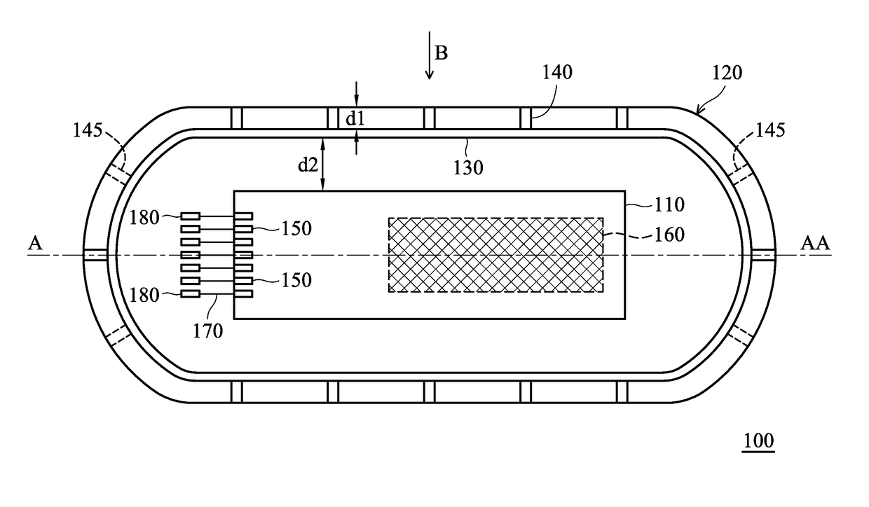
[0019]FIG. 1 shows a top view of a fingerprint sensor 100 according to an embodiment of the invention. In FIG. 1, a molding compound of the fingerprint sensor 100 is removed to simplify the description, wherein the molding compound of the fingerprint sensor 100 will described in FIG. 2 and FIG. 3. Referring to FIG. 1, the fingerprint sensor 100 comprises a sensing die 110, a printed circuit board (PCB) 120, an electrostatic discharge (ESD) ring 130, and a plurality of metal stubs 140 and 145. In general, the sensing die 110 comprises a sensing array, a readout module, a processor and so on. In the sensing die 110, after obtaining a sensing output of the sensing array, ...


PUM


Abstract

A fingerprint sensor is provided. The fingerprint sensor includes a sensing array sensing fingerprint information of a user, an insulating surface disposed on the sensing array, and a printed circuit board (PCB) disposed under the sensing array. The PCB includes a substrate, a ground plane disposed on the second surface of the substrate, and an electrostatic discharge (ESD) ring disposed on the first surface of the substrate and surrounding the sensing array. The substrate includes a first surface and a second surface opposite the first surface. The ESD ring surrounds the sensing array. When an ESD event occurs, ESD energy is discharged from the ESD ring to the ground plane through a plurality of vias in the substrate without passing the sensing array.

Description

CROSS REFERENCE TO RELATED APPLICATIONS[0001]This application claims priority of China Patent Application No. 201510351738.7, filed on Jun. 24, 2015, the entirety of which is incorporated by reference herein.BACKGROUND OF THE INVENTION[0002]Field of the Invention[0003]The invention relates to a fingerprint sensor, and more particularly to a fingerprint sensor that is protected from electrostatic discharge (ESD).[0004]Description of the Related Art[0005]In recent years, biological identification technology has become increasingly mature, and different biological features can be used for identifying users. Since the recognition rate and accuracy of fingerprint identification technology are better than those of other biological feature identification technologies, fingerprint identification and verification are used extensively in various areas.[0006]Fingerprint identification and verification technology detects a user's fingerprint pattern, captures fingerprint data from the fingerpri...

Claims


Application Information

Patent Timeline
Patent Type & Authority Patents(United States)
IPC IPC(8): G06K9/00H05F3/02H05K1/02H05K1/11
CPCH05F3/02G06K9/00053H05K1/0254H05K1/115H05K2201/1031H05K2201/10151G06V40/1306H05K1/0215H05K1/0259G06V40/1329
Inventor WANG, CHENG-CHUNG
Owner EGIS TECH
Features
  • R&D
  • Intellectual Property
  • Life Sciences
  • Materials
  • Tech Scout
  • Unparalleled Data Quality
  • Higher Quality Content
  • 60% Fewer Hallucinations
Learn More