
Conductive sheet, touch panel, display device, method for producing said conductive sheet, and non-transitory recording medium

a technology of conductive sheets and display devices, which is applied in the direction of conductive layers on insulating supports, instruments, other domestic articles, etc., can solve the problems of graininess or roughness, etc., and achieve the effect of easy to sense graininess or roughness, and easy to be seen by users

Active Publication Date: 2017-05-02
FUJIFILM CORP
View PDF46 Cites 4 Cited by
  • Summary
  • Abstract
  • Description
  • Claims
  • Application Information

AI Technical Summary

Benefits of technology

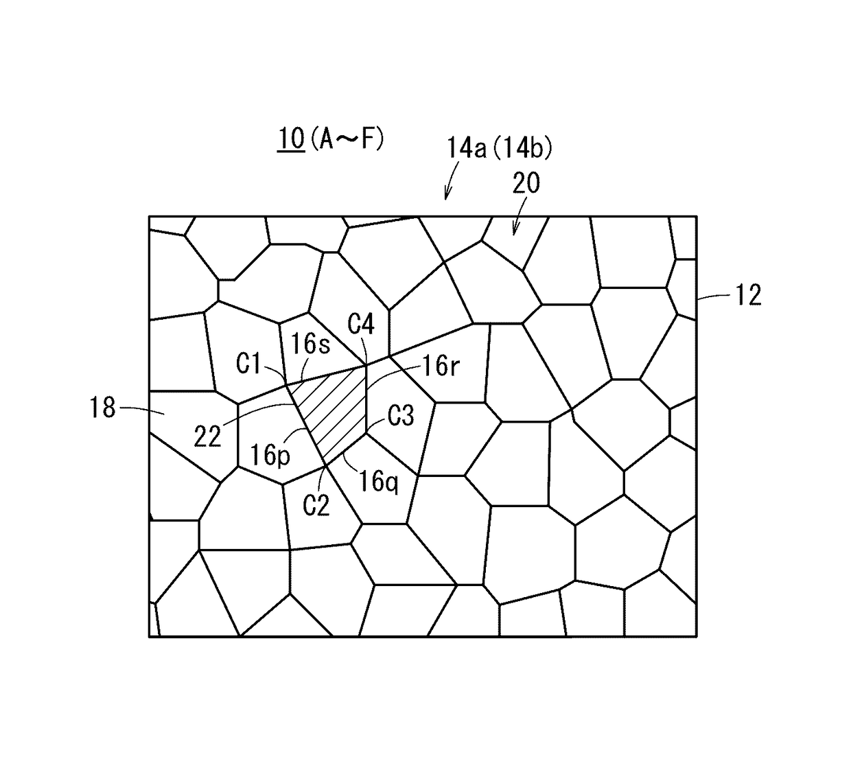
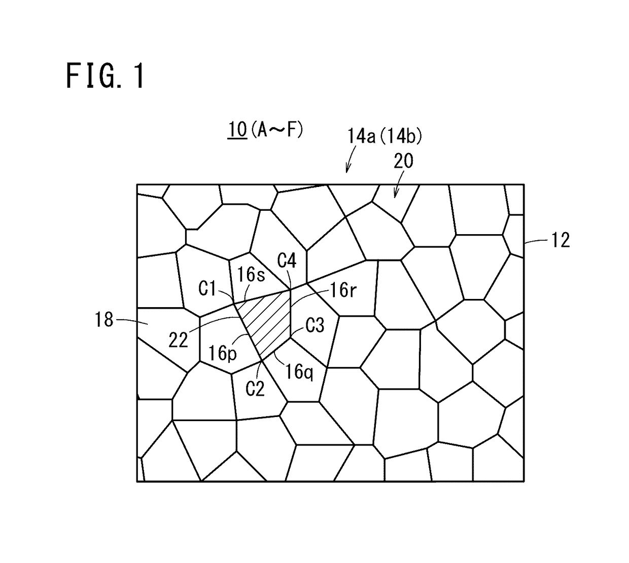
[0010]However, in the case of using a metal, which is a non-translucent material, as the electrode of a touch panel, a difference in the amount of light transmitted through the electrode in accordance with the presence or absence of the thin metal wires is increased. Thus, shading corresponding to the shape of the pattern formed by the electrode becomes significant, which is easily visible to the user. In particular, in the case of a mesh pattern in which different mesh shapes are arranged without gaps therebetween, there is a disadvantage in that sensation of graininess or roughness (grain noise) occurs easily.
[0011]The present invention has been made with a view toward solving the aforementioned problems. An object of the present invention is to provide a conductive sheet, a touch panel and a display device, a method for producing the conductive sheet, and a non-transitory recording medium, in which the occurrence of a sensation of roughness (graininess) caused by the pattern can be suppressed, and wherein the visibility of an object to be observed, i.e., an observation target, can be improved significantly.

Problems solved by technology

In particular, in the case of a mesh pattern in which different mesh shapes are arranged without gaps therebetween, there is a disadvantage in that sensation of graininess or roughness (grain noise) occurs easily.

Method used


Image

  • Conductive sheet, touch panel, display device, method for producing said conductive sheet, and non-transitory recording medium
  • Conductive sheet, touch panel, display device, method for producing said conductive sheet, and non-transitory recording medium
  • Conductive sheet, touch panel, display device, method for producing said conductive sheet, and non-transitory recording medium

Examples


example applied

[Example Applied to Resistive Film Type Touch Panel]

[0407]The present invention can be applied not only to an electrostatic capacitance type, but also to a resistive film type (as well as to a digital type, or an analog type) of touch panel 160. Below, with reference to FIGS. 51 to 53, the structure and operational principles of such a touch panel 160 will be described.

[0408]A digital resistive film type touch panel 160 comprises a lower side panel 162, an upper side panel 164 arranged in confronting relation to the lower side panel 162, a frame adhesive layer 166 bonded to peripheral edge portions of the lower side panel 162 and the upper side panel 164, and which serves to electrically insulate both the panels from each other, and an FPC 168 (Flexible Printed Circuit) sandwiched between the lower side panel 162 and the upper side panel 164.

[0409]As shown in FIG. 51 and FIG. 52A, the upper side panel 164 includes a first transparent substrate 170a made from a flexible material (e.g...

##ventive example 1

Inventive Example 1

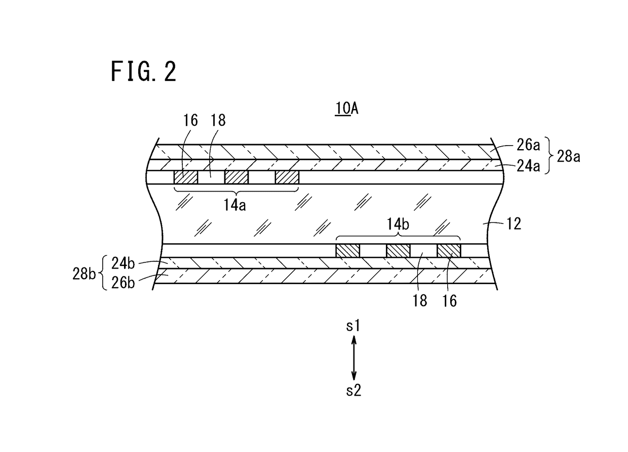
[0490]A conductive sheet 10 according to the first inventive example was manufactured using polychlorotrifluoroethylene (PCTFE) with an index of refraction n1=1.42 as the first protective layer 26a. In this case, the relative index of refraction nr1 was nr1=(1.42 / 1.64)=0.86.

##ventive example 2

Inventive Example 2, Comparative Examples 1 to 3

[0491]A conductive sheet 10 according to the second inventive example was manufactured using polymethyl methacrylate (PMMA) with an index of refraction n1=1.50 as the first protective layer 26a. In this case, the relative index of refraction nr1 was nr1=(1.50 / 1.64)=0.91.

[0492]Further, concerning comparative example 1 corresponding to the pattern PT1 (see FIG. 57A), comparative example 2 corresponding to the pattern PT2 (see FIG. 57B), and comparative example 3 corresponding to the pattern PT3 (see FIG. 57C), respective samples were made by covering the aforementioned patterns with polymethyl methacrylate.

Inventive Example 3, Inventive Example 7

[0493]Conductive sheets 10 according to the third and seventh inventive examples were manufactured using polystyrene (PS) with an index of refraction n1=1.60 as the first protective layer 26a. In this case, the relative index of refraction nr1 was nr1=(1.60 / 1.64)=0.97.


PUM

PropertyMeasurementUnit
widthaaaaaaaaaa
widthaaaaaaaaaa
widthaaaaaaaaaa

Abstract

The present invention pertains to: a conductive sheet, a touch panel, a display device, a method for producing the conductive sheet, and a recording medium. In the present invention, the relative refractive index of a substrate with respect to a first protective layer, and / or the relative refractive index of the substrate with respect to a second protective layer is 0.86-1.15. The relative refractive index of a first substrate with respect to the first protective layer, and / or the relative refractive index of a second substrate with respect to the second protective layer is 0.86-1.15.

Description

CROSS-REFERENCE TO RELATED APPLICATIONS AND PRIORITY CLAIMS[0001]This application is a Continuation of International Application No. PCT / JP2012 / 067620 filed on Jul. 10, 2012, which was published under PCT Article 21(2) in Japanese, which is based upon and claims the benefit of priority from Japanese Patent Applications No. 2011-152534 filed on Jul. 11, 2011, No. 2011-152759 filed on Jul. 11, 2011, No. 2011-193505 filed on Sep. 6, 2011, and No. 2011-193506 filed on Sep. 6, 2011, the contents all of which are incorporated herein by reference.TECHNICAL FIELD[0002]The present invention relates to a conductive sheet, a touch panel and a display device, a method for producing the conductive sheet, and a non-transitory recording medium.BACKGROUND ART[0003]Recently, electronic devices that incorporate touch panels therein have been spreading widely. Touch panels are mounted in many devices including small screen, such as portable phones, PDAs (Personal Digital Assistants), or the like. In t...

Claims


Application Information

Patent Timeline
Patent Type & Authority Patents(United States)
IPC IPC(8): G06F3/041B32B7/02B32B15/02G06F3/044B32B27/40H05K1/02B32B27/32B32B27/30B32B15/08G06F1/16B32B7/023
CPCH05K1/0298B32B7/02B32B15/02B32B15/08B32B27/302B32B27/32B32B27/40G06F1/1692G06F3/044B32B2457/208G06F2203/04103B32B2307/202B32B2307/412B32B2307/418G06F2203/04111G06F3/0446G06F3/0445B32B7/023G06F3/041H01B5/14
Inventor IWAMI, KAZUCHIKAISHIBASHI, HIDEYASUWAKUI, TAKASHI
Owner FUJIFILM CORP
Learn More