Check patentability & draft patents in minutes with Patsnap Eureka AI!

Memory interface system

a memory interface and interface technology, applied in the field of memory interface systems, can solve the problems of affecting system performance, delay elements may add delays to data strobes, and may increase data requests, so as to reduce or no delay data requests, the effect of less handshaking

Active Publication Date: 2017-07-04
APPLE INC
View PDF19 Cites 0 Cited by
  • Summary
  • Abstract
  • Description
  • Claims
  • Application Information

AI Technical Summary

Benefits of technology

This approach enables quicker processing of memory requests and reduced delays by storing configuration data locally, allowing the memory interface system to operate more efficiently and mitigate potential deadlocks during state changes.

Problems solved by technology

As clock speeds increase, inherent delays between the data strobe and the data may cause errors.
Such delays may be exacerbated by voltage and temperature variations.
In some cases, delay elements may add delays to the data strobe, the data signals, or both to align the data strobe to the data signals.
However, calibrating the delay elements may occupy resources that could otherwise be used by the memory system, which may negatively affect system performance.
Further, in some embodiments, because the memory device may be unable to service requests while transitioning to the second frequency, issuing the configuration data from the memory controller to the memory interface circuit in response to the memory device transitioning to the second frequency may result in reduced or no delay to data requests to the memory device due to the issuing the configuration data.

Method used


Image

  • Memory interface system
  • Memory interface system
  • Memory interface system

Examples


Embodiment Construction

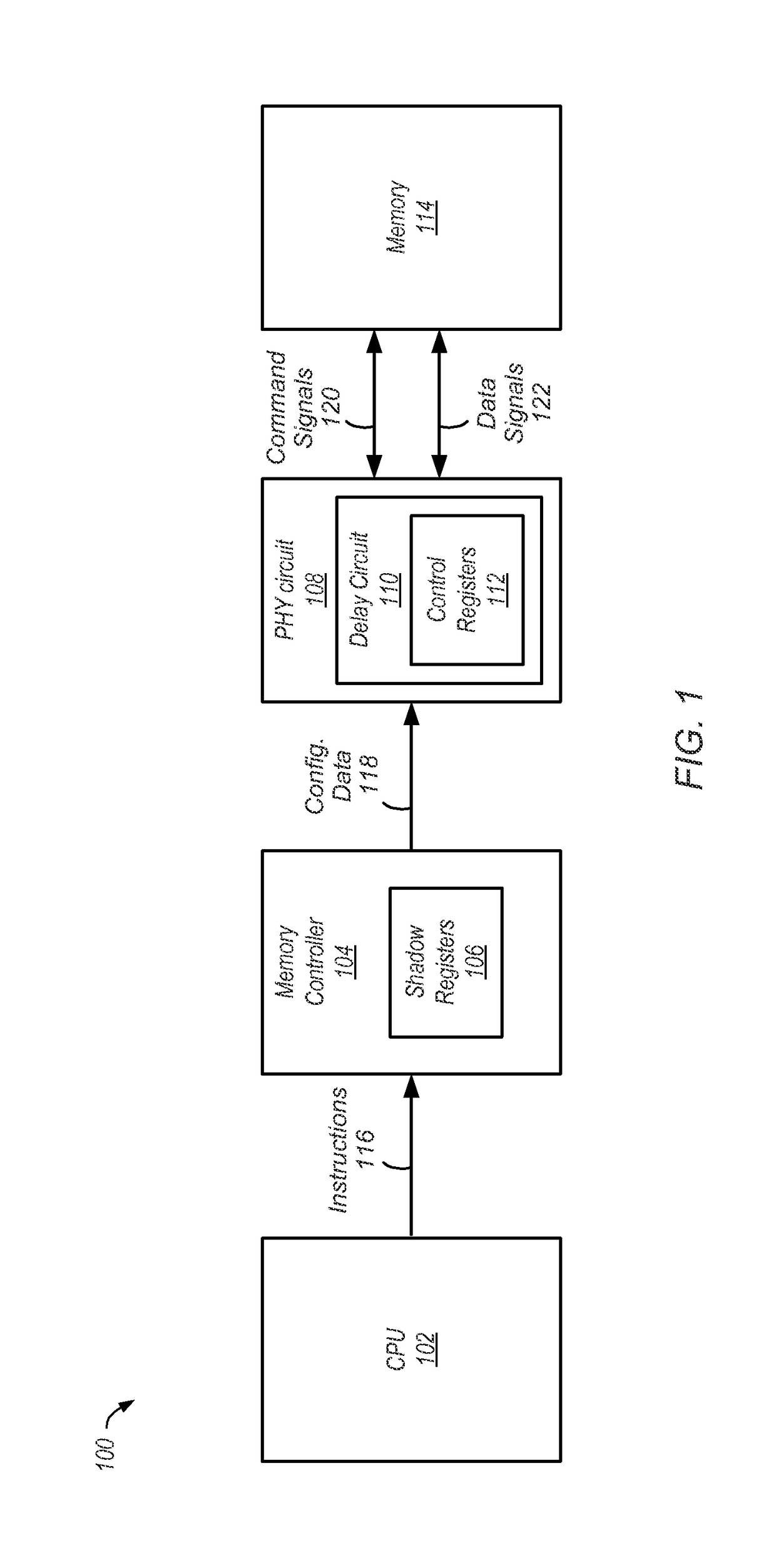
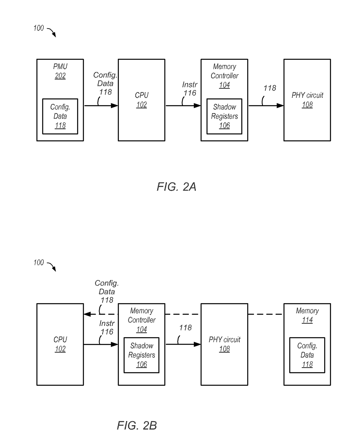
[0018]As described above, a memory interface system that includes a memory controller and a physical layer (PHY) circuit may provide memory requests to a memory device. Additionally, the PHY circuit may store configuration information used to facilitate communications with the memory device (e.g., delay information used to synchronize signals between the PHY circuit and the memory device). The memory device may be configured to operate differently during a first system state, as compared to a second system state (e.g., a state where the memory device operates at a first frequency and a state where the memory device operates at a second, higher, frequency). In some embodiments, the PHY circuit may use different configuration information to facilitate communications with the memory device when the memory device is operating during the first system state, as compared to the second system state. In some cases, the PHY circuit may be unable to communicate with the memory device until it ...


PUM


Abstract

In some embodiments, a memory interface system includes a memory interface circuit and a memory controller. The memory interface circuit is configured to communicate with a memory device. The memory controller is configured, in response to the memory device operating at a first frequency, to store configuration information corresponding to the memory device operating at a second frequency. The memory controller is further configured, in response to the memory device transitioning to the second frequency, to send the configuration information to the memory interface circuit. In some embodiments, storing the configuration information may result in some memory requests being provided to the memory device more quickly, as compared to a different memory interface system where the configuration information is not stored at the memory controller. Additionally, in some embodiments, storing the configuration information may result in the configuration information being transmitted to the memory interface circuit more efficiently.

Description

BACKGROUND[0001]Technical Field[0002]This disclosure relates generally to a memory interface system.[0003]Description of the Related Art[0004]In many memory systems, such as various double data rate (DDR) systems, a clock signal known as a data strobe is transmitted along with data signals. Data signals received at the memory may be synchronized to the data strobe.[0005]As clock speeds increase, inherent delays between the data strobe and the data may cause errors. Such delays may be exacerbated by voltage and temperature variations. In some cases, delay elements may add delays to the data strobe, the data signals, or both to align the data strobe to the data signals. However, calibrating the delay elements may occupy resources that could otherwise be used by the memory system, which may negatively affect system performance.SUMMARY[0006]In various embodiments, a memory interface system is disclosed that includes a memory interface circuit and a memory controller. The memory interfac...

Claims


Application Information

Patent Timeline
Patent Type & Authority Patents(United States)
IPC IPC(8): G06F12/00G11C7/10G06F12/06G06F12/02G06F13/28G06F13/00G11C8/18G11C29/02G06F13/16
CPCG06F13/161G06F12/023G06F12/0646G11C7/1072G11C8/18G11C29/022G11C29/023G11C29/028G06F2212/1044G11C7/1045G11C7/1066
Inventor JETER, ROBERT E.PARIK, NEERAJ
Owner APPLE INC
Features
  • R&D
  • Intellectual Property
  • Life Sciences
  • Materials
  • Tech Scout
  • Unparalleled Data Quality
  • Higher Quality Content
  • 60% Fewer Hallucinations
Learn More